Display device and method for driving the same

Active Publication Date: 2006-03-02
SHARP KK
View PDF7 Cites 55 Cited by
  • Summary
  • Abstract
  • Description
  • Claims
  • Application Information

AI Technical Summary

Benefits of technology

[0023] The present invention is designed to solve the foregoing problems and has as an object to realize a display device which makes it possible to

Problems solved by technology

However, the foregoing problem occurs more conspicuously.
This raises a prob

Method used


Image

  • Display device and method for driving the same
  • Display device and method for driving the same
  • Display device and method for driving the same

Examples


first embodiment

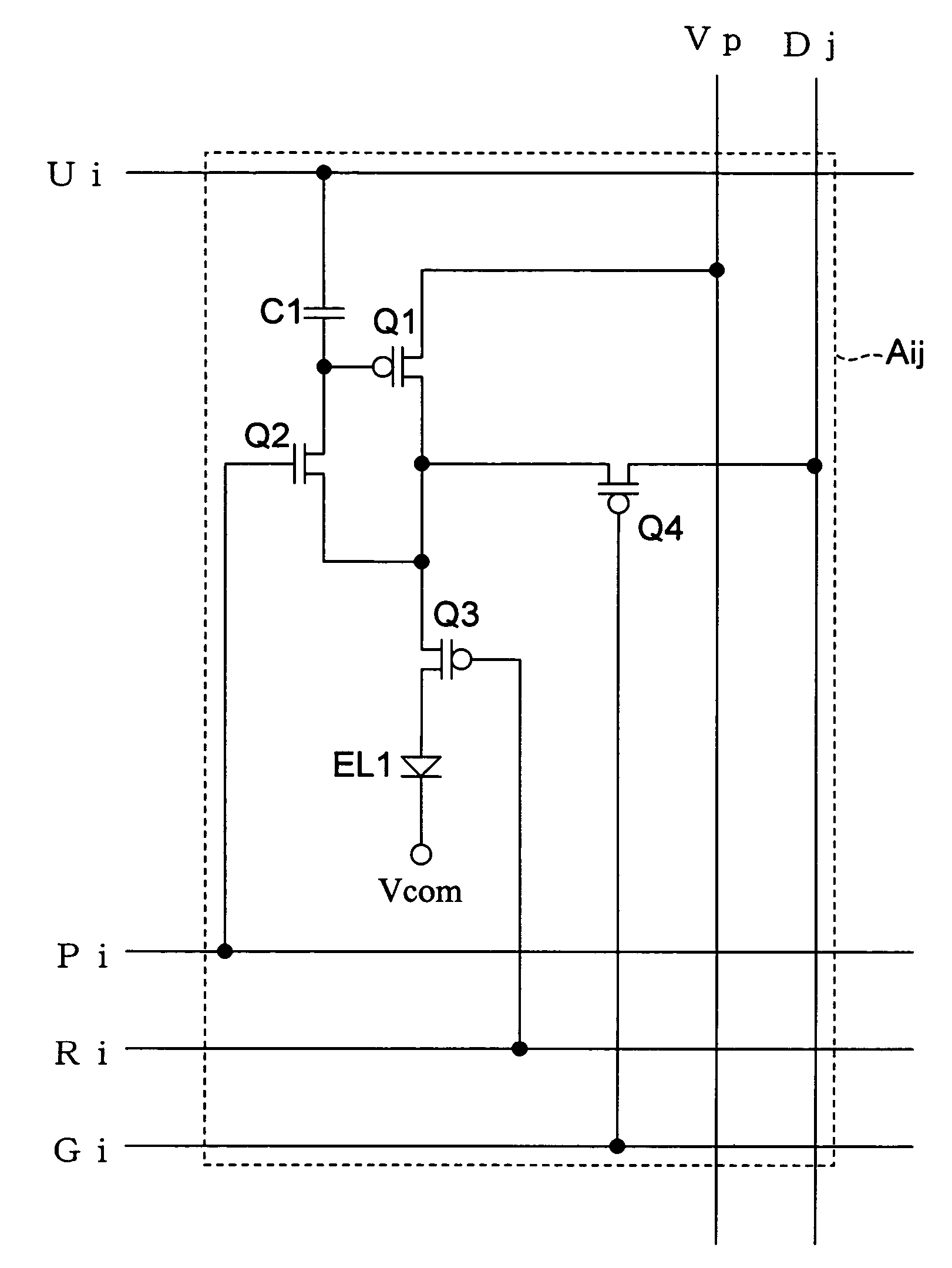
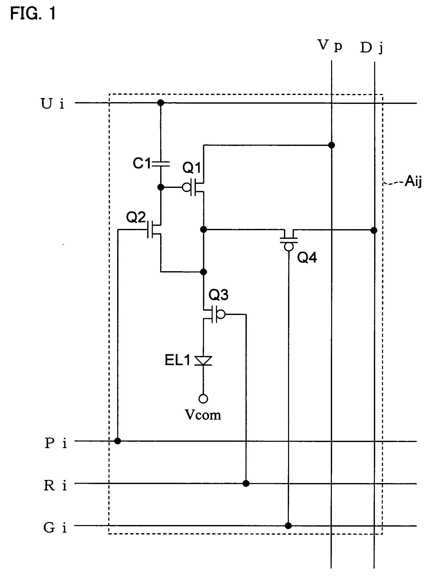
[0060] In the present embodiment, a first example of a display device of the present invention will be described.

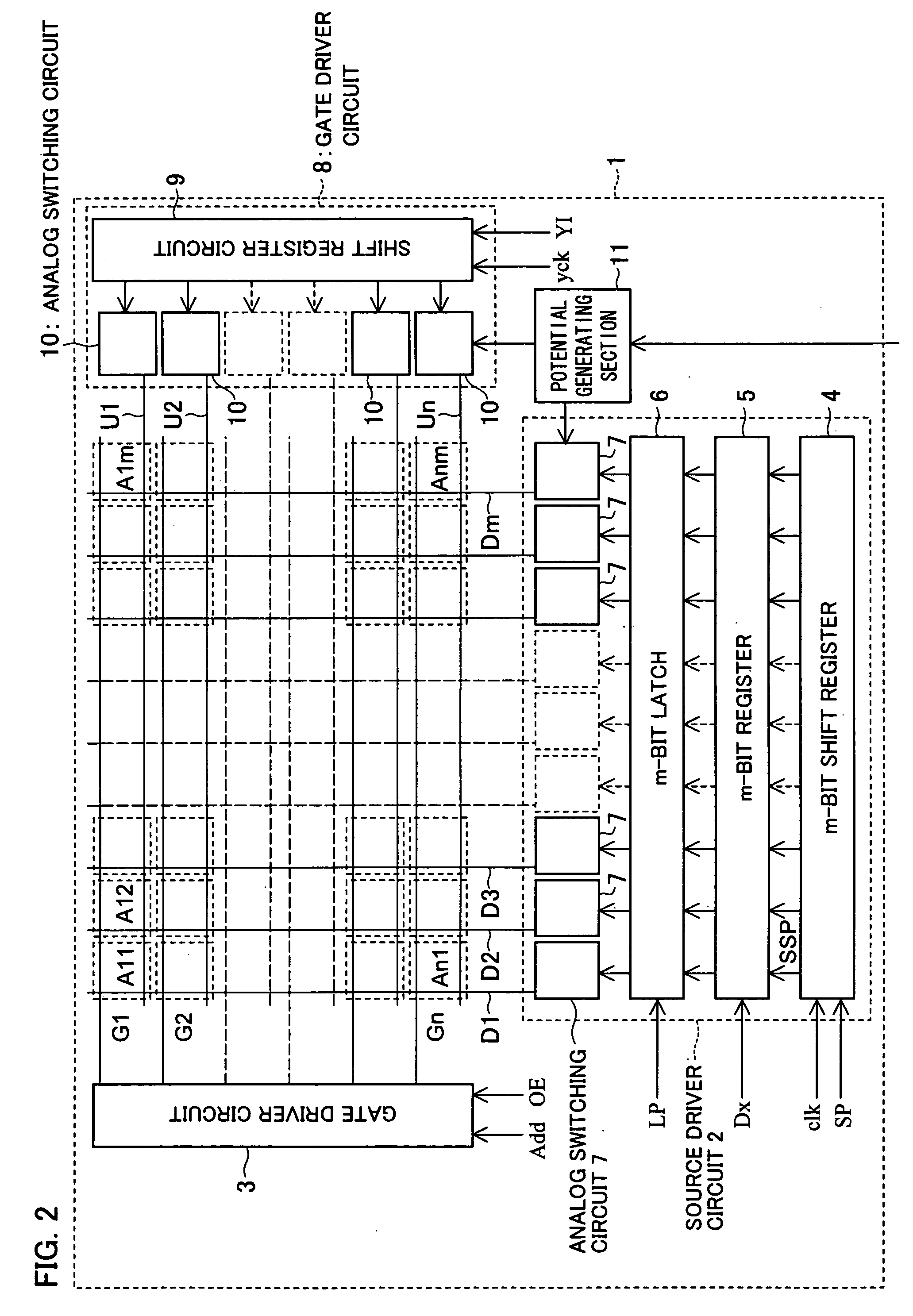
[0061] A display device1 of the present embodiment, as shown in FIG. 2, has pixel circuits Aij (i=1 to n, j=1 to m), gate drivers 3 and 8, a source driver 2, and a potential generating section 11. The pixel circuits Aij are disposed in a matrix manner. The gate drivers 3 and 8 and a source driver circuit 2 serve as a wiring control circuit for the pixel circuits Aij. The potential generating section 11 serves as an internal voltage generating circuit.

[0062] Each of the pixel circuits Aij is disposed in a region where a data wire Dj and a gate wire Gi intersect with each other. Further, the source driver circuit 2 includes an m-bit shift register 4, an m-bit register 5, an m-bit latch 6, and m-number of analog switch circuits 7.

[0063] In the source driver circuit 2, a first register of the m-bit shift register 4 receives a start pulse SP, and the start pulse SP is trans...

second embodiment

[0116] In the present embodiment, a second example of the display device according to the present invention will be described.

[0117] Since a display device 1 according to the present embodiment also has the same arrangement as shown in FIG. 2, the description is omitted.

[0118]FIG. 11 shows an arrangement of a pixel circuit Aij according to the present embodiment.

[0119] The pixel circuit Aij has an n-type switching TFT: Q5 (fourth switching transistor) disposed between a gate terminal (current control terminal) of a driving TFT: Q1 (driving transistor) and a data wire Dj instead of the switching TFT: Q4 (third switching transistor) of the pixel circuit Aij of FIG. 1. Since the pixel circuit of FIG. 11 is the same as the pixel circuit of FIG. 1 otherwise, a further description thereof is omitted here.

[0120] Operation of the pixel circuit Aij will be described below with reference to a timing chart of FIG. 12.

[0121] In FIG. 12, Ui, G1, Ri, and Pi correspond to the pixel circuit Ai...

third embodiment

[0143] In the present embodiment, a third example of the display device according to the present invention will be described.

[0144] Since a display device 1 according to the present embodiment also has the same arrangement as shown in FIG. 2, the description thereof is omitted.

[0145]FIG. 15 shows an arrangement of a pixel circuit Aij according to the present embodiment.

[0146] The pixel circuit Aij has a capacitor C3 (second capacitor) provided between a drain terminal (current output terminal) of a driving TFT: Q1 (driving transistor) and a data wire Dj instead of the switching TFT: Q4 (third switching transistor) of the pixel circuit Aij of FIG. 1. Further, the gate wire Gi for controlling a gate voltage of the switching TFT: Q4 is also removed. Since the pixel circuit of FIG. 15 is the same as the pixel circuit of FIG. 1 otherwise, a further description thereof is omitted here.

[0147] Operation of the pixel circuit Aij will be described below with reference to a timing chart of...


PUM


Abstract

A display device which makes it possible to shorten a selection period per pixel while compensating variations in a threshold voltage of the driving transistor, and a method for driving the same are achieved. In a pixel circuit Aij, a potential wire Ui is set to a potential Vcc, a voltage of a gate wire Gi becomes Low, a voltage of a control wire Ri becomes High, and a voltage of a control wire Pi becomes High, so that a gate terminal of a driving TFT: Q1 has a potential of a data wire Dj. Moreover, a voltage of the gate wire Gi becomes High so as to compensate a threshold voltage of the driving TFT: Q1. Thereafter, a voltage of the control wire Pi becomes Low, and the potential wire Ui is set to a potential Vc, so that a voltage of a capacitor C1, i.e., a gate-source voltage of the driving TFT is changed. This causes a voltage of the control wire Ri to be Low, so that a driving current is flown into an organic EL: EL1.

Description

[0001] This Nonprovisional application claims priority under 35 U.S.C. § 119(a) on Patent Application No. 2004 / 254615 filed in Japan on Sep. 1, 2004, the entire contents of which are hereby incorporated by reference. FIELD OF THE INVENTION [0002] The present invention relates to a display device using a current-driven electro-optic element such as an organic EL (electroluminescence) display or an FED (field emission display). The present invention also relates to a method for driving the display device. BACKGROUND OF THE INVENTION [0003] Recently, research and development of a current-driven light-emitting element such as an organic EL (electroluminescence) display or an FED have been actively carried out. Particularly, an organic EL display is a display which can emit light at low voltage and with low power consumption, and draws attention as being used for a mobile device such as a mobile phone or a PDA (personal digital assistance). [0004] As an arrangement of a current-driven pi...

Claims


Application Information

Patent Timeline
IPC IPC(8): G09G3/36
CPCG09G3/3233G09G2300/0819G09G2300/0842G09G2320/043G09G2300/0861G09G2300/0866G09G2300/0876G09G2300/0852
Inventor NUMAO, TAKAJI
Owner SHARP KK
Why Eureka
Try Eureka