

Image pickup device and image pickup system
a pickup device and image technology, applied in the field of image pickup devices and image pickup systems, can solve the problems of difficult to leave an adequate area for the photodiode and the image quality is deteriorating considerably, and achieve the effect of preventing blooming
- Summary
- Abstract
- Description
- Claims
- Application Information
AI Technical Summary
Benefits of technology
Problems solved by technology
Method used
Image

Examples
first embodiment
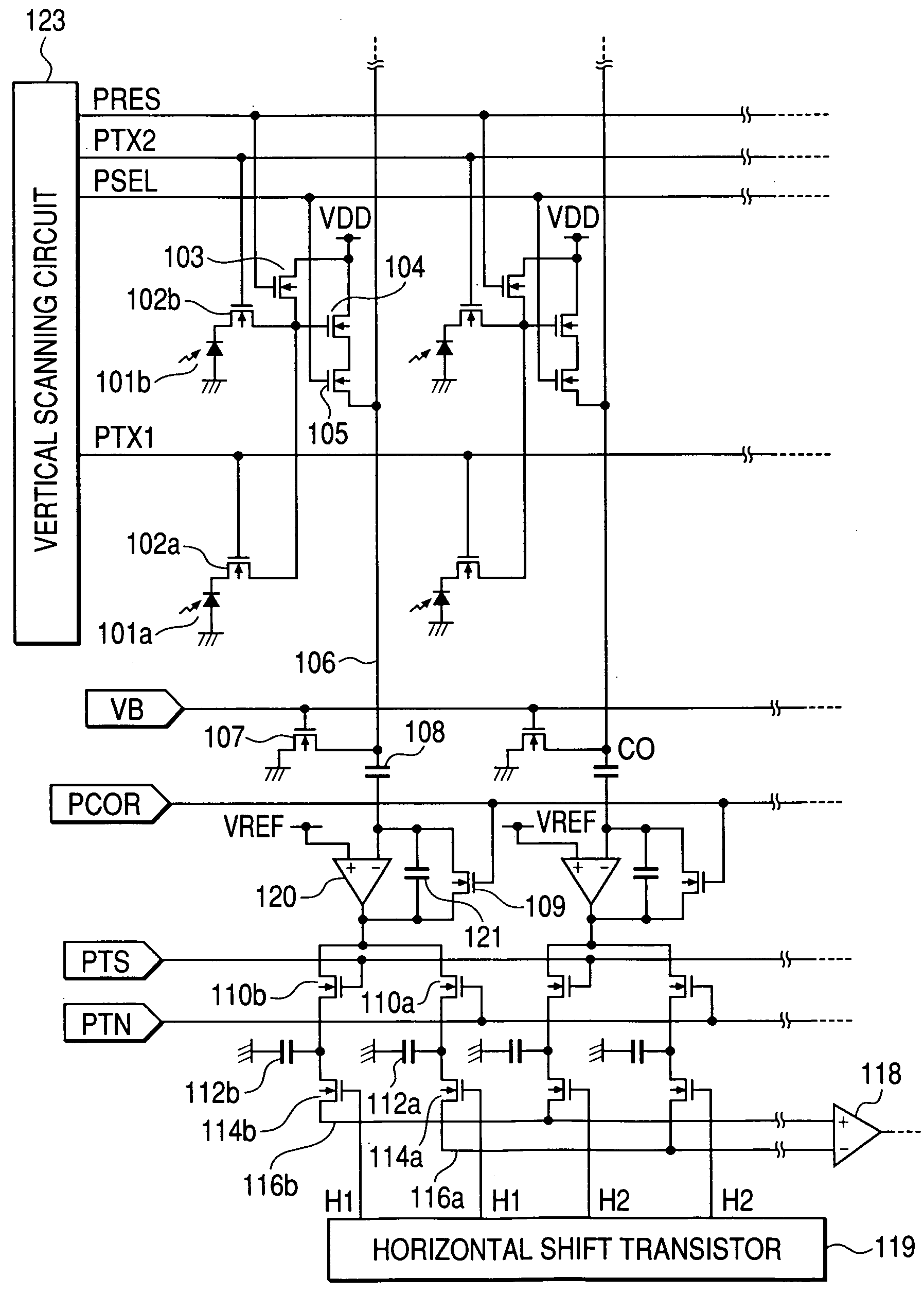
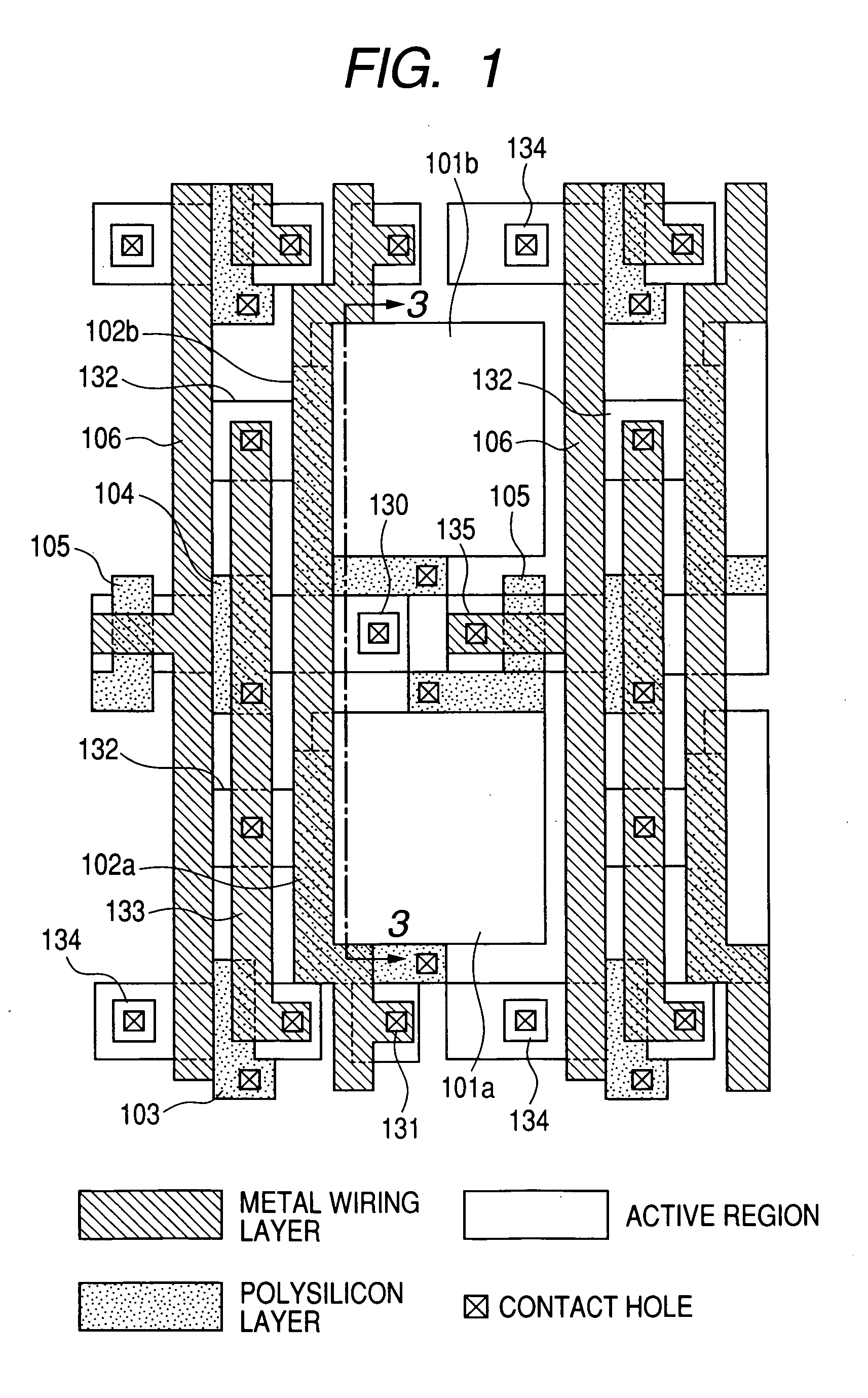
[0031] Here, an image pickup device according to a first embodiment of the present invention will be described. FIG. 1 is a plan view showing unit cells in a solid image pickup device according to a first embodiment. FIG. 2 is a view showing an equivalent circuit of the image pickup device according to this embodiment, in which pixels having a layout shown in FIG. 1 are arranged in two-dimensional pattern (matrix pattern). It is not necessary that the pixels are arranged in the matrix pattern strictly, but, for example, the pixels may be arranged in a honeycomb pattern (see Japanese Patent Application Laid-Open No. 2000-077344).
[0032] In FIG. 2, each unit cell includes photodiodes 101a and 101b as photoelectric conversion elements, an amplifying MOSFET 104 as a common amplifying means for amplifying signals generated by the photodiodes 101a and 101b; and a reset MOSFET 103 as a common reset switch for resetting an input of the amplifying MOSFET 104 to predetermined voltage. In addi...
second embodiment
[0042] Next, an image pickup device according to a second embodiment of the present invention will be explained. FIG. 7 is a view showing an equivalent circuit of an image pickup device according to the second embodiment and illustrating a part relating to 2×4 pixels among pixels arranged in a two-dimensional pattern. In the image pickup device according to the second embodiment, four pixels hold the amplifying MOSFET, reset MOSFET and row election MOSFET in common, thereby constituting a unit cell. FIG. 8 is a plan view showing a layout of these pixels. In FIGS. 7 and 8, constructional members same as those in FIGS. 2 and 1 are designated by the same reference numerals and duplicated explanation will be omitted. Although a configuration of a gate electrode of a transfer MOSFET of FIG. 8 is different from the gate electrode of the pixel transfer MOSFET of FIG. 1 apparently, such difference is generated by simplifying the Figure and the actual configuration of the gate electrode of t...
third embodiment
[0045] Next, an image pickup device according to a third embodiment of the present invention will be explained. An equivalent circuit of the image pickup device according to the third embodiment is similar to that in the second embodiment. FIG. 9 is a plan view showing a layout of pixels. In FIG. 9, constructional members same as those in FIG. 8 are designated by the same reference numerals and duplicated explanation will be omitted. Four pixels hold a reset MOSFET 103, an amplifying MOSFET 104 and a row election MOSFET 105 in common and the photodiodes 101a, 101b, 101c and 101d are disposed in 4n-3, 4n-2, 4n-1 and 4n rows, respectively (here, n is the natural number). The transfer MOSFETs 102a, 102b, 102c and 102d are disposed in correspondence to the photodiodes 101a, 101b, 101c and 101d, respectively. Similar to the image pickup device of the second embodiment, a drain region 130 of the amplifying MOSFET 104 connected to the power source, a drain region 134 of the reset switch 10...
PUM
 Abstract
Description
Claims
Application Information