Optical printed circuit board and optical interconnection block using optical fiber bundle

a technology of optical interconnection block and printed circuit board, which is applied in the direction of circuit optical details, optical elements, instruments, etc., can solve the problems of optical fiber, difficult to accurately match, etc., and achieve the effect of increasing the tolerance of misalignmen

Inactive Publication Date: 2006-03-02
INFORMATION & COMM UNIV RES & INDAL COOPERATION GROUP +1
View PDF5 Cites 148 Cited by
  • Summary
  • Abstract
  • Description
  • Claims
  • Application Information

AI Technical Summary

Benefits of technology

[0018] It is an advantage of the present invention to provide an optical PCB using an optical fiber bundle, and an optical interconnection block for increasing the tolerance of misalignment without using a single optical fiber for each channel.
[0019] It is another advantage of the present invention to provide an optical PCB using an optical fiber bundle, and an optical interconnection block for using an optical fiber bundle in a multi-layered optical PCB and an optical interconnection block to generate optical waveguides once, instead of individually generating the optical waveguides.
[0020] In one aspect of the present invention, an optical printed circuit board (PCB) having a multi-channel optical waveguide comprises: an optical waveguide having an optical path for transmitting light beams; a groove for penetrating the optical waveguide; and an optical interconnection block inserted in the groove and connected to the optical waveguide to transmit the light beams, wherein the optical interconnection block includes an optical fiber bundle bent by the angle of 90°.
[0021] The optical interconnection block connects a plurality of multi-layered optical waveguides to transmit light beams to the optical waveguides.
[0022] A diameter of a core of an optical fiber ranges from 0.5 to 20 μm.
[0023] A radius of inside curvature of the optical fiber bundle ranges from 0.1 to 10 mm within the thickness of the optical PCB.

Problems solved by technology

However, it is difficult to accurately match the position of the optical fiber 8 or 14 in the optical interconnection block with the position of the optical waveguide 2 of the optical PCB 1 since the optical interconnection blocks are connected with a single optical fiber for each optical signal channel.

Method used


Image

  • Optical printed circuit board and optical interconnection block using optical fiber bundle
  • Optical printed circuit board and optical interconnection block using optical fiber bundle
  • Optical printed circuit board and optical interconnection block using optical fiber bundle

Examples


Embodiment Construction

[0038] In the following detailed description, only the preferred embodiment of the invention has been shown and described, simply by way of illustration of the best mode contemplated by the inventor(s) of carrying out the invention. As will be realized, the invention is capable of modification in various obvious respects, all without departing from the invention. Accordingly, the drawings and description are to be regarded as illustrative in nature, and not restrictive. To clarify the present invention, parts which are not described in the specification are omitted, and parts for which same descriptions are provided have the same reference numerals.

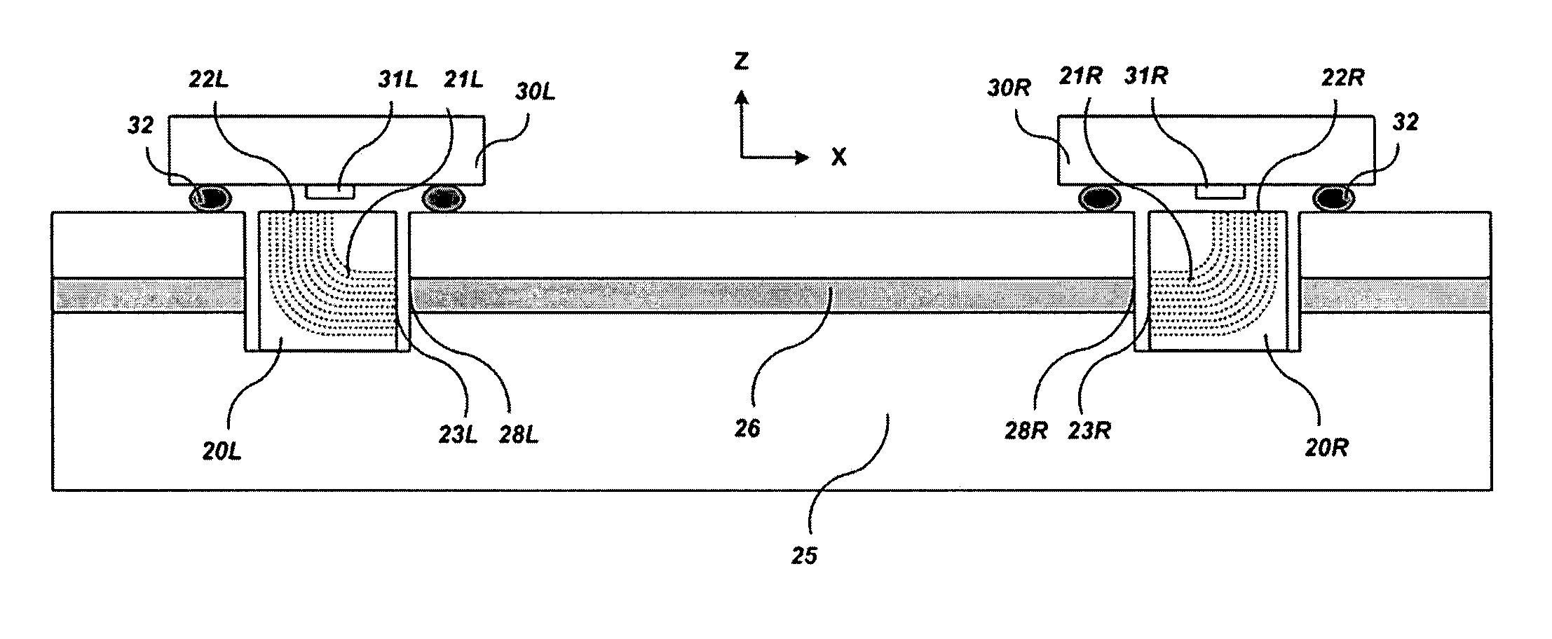
[0039]FIG. 3A shows an optical interconnection block using an optical fiber bundle bent by the angle of 90° according to an exemplary embodiment of the present invention, and FIG. 3B shows a cross-sectional view (a top surface 22 or a side surface 23) of an optical interconnection block using an optical fiber bundle according to an exemp...


PUM


Abstract

Disclosed is an optical printed circuit board (PCB) having a multi-channel optical waveguide, which comprises: an optical waveguide having an optical path for transmitting light beams; a groove for penetrating the optical waveguide; and an optical interconnection block inserted in the groove and connected to the optical waveguide to transmit the light beams, wherein the optical interconnection block includes an optical fiber bundle bent by the angle of 90°. The optical interconnection block connects a plurality of multi-layered optical waveguides to transmit light beams to the optical waveguides. The optical fiber bundle is installed as a medium of the multi-channel optical waveguide in the optical PCB.

Description

CROSS REFERENCE TO RELATED APPLICATION [0001] This application claims priority to and the benefit of Korea Patent Application No. 10-2004-67105 filed on Aug. 25, 2004 in the Korean Intellectual Property Office, the entire content of which is incorporated herein by reference. BACKGROUND OF THE INVENTION [0002] (a) Field of the Invention [0003] The present invention relates to an optical printed circuit board (PCB) and an optical interconnection block using an optical fiber bundle. More specifically, the present invention relates to an optical printed circuit board with a built-in optical waveguide, and an optical interconnection block in optical PCB based optical interconnectors. [0004] (b) Description of the Related Art [0005] In general, a printed circuit board (PCB) represents a phenol-resin or epoxy-resin circuit board on which various components are mounted and paths for interconnecting the components are fixedly printed. As to a PCB manufacturing process, a thin film of copper ...

Claims


Application Information

Patent Timeline
Patent Type & Authority Applications(United States)
IPC IPC(8): G02B6/42G02B6/26H05K1/11H05K1/16
CPCG02B6/06H05K1/0274G02B6/43H05K1/11H05K1/16
Inventor CHO, MU HEECHO, HAN SEOPARK, HYO HOONLEE, JONG HOKIM, KYUNG ROK
Owner INFORMATION & COMM UNIV RES & INDAL COOPERATION GROUP
Why Eureka
Try Eureka