Output power error absorbing circuit and multi-carrier transmitter having the same

a technology of output power error and multi-carrier transmitter, which is applied in the direction of multi-channel communication, digital transmission, transmission, etc., can solve the problems of output power error, number of carriers, distortion of transmission signals, etc., and achieve the effect of improving the efficiency of power amplifiers

Inactive Publication Date: 2006-03-02
FUJITSU LTD
View PDF3 Cites 23 Cited by
  • Summary
  • Abstract
  • Description
  • Claims
  • Application Information

AI Technical Summary

Benefits of technology

[0022] It is preferable that the power correction value generating unit comprises a reference output power value table which outputs the reference output power value beforehand obtained for each of the carrier settings differing from one another, a difference arithmetic unit which obtains difference information between the reference output power value outputted from the reference output power value table and a multiplexed power value of the carrier signals before undergone the peak suppression, a PAR table which outputs PAR information about a ratio of peak to average power beforehand obtained for each of the peak suppression settings differing from one another and each of the carrier settings differing from one another, an adder which adds the PAR information from the PAR table under the peak suppression setting and the carrier setting to the difference information obtained by the difference arithmetic unit, and outputs a result of the addition as present PAR information, and a correction value table which outputs a power correction value for minimizing the error beforehand obtained for the PAR information from the adder as a correction value used for gain correction by the output power error correcting unit to the output power error correcting unit.
[0023] The present invention further provides a multi-carrier transmitter with an output power error absorbing function, comprising a carrier multiplexing unit which multiplexes a plurality of carrier signals, a peak power suppressing unit which suppresses a peak power generating in a multiplexed signal which is an output of the carrier multiplexing unit by correcting a gain of each of the carrier signals before multiplexed by the carrier multiplexing unit according to a peak suppression setting, and an output power error absorbing circuit which corrects a signal gain before or after the multiplexing by the carrier multiplexing unit based on a carrier setting relating to either one or both of the number of the carrier signals and frequency arrangement, and the peak suppression setting so that an error from a reference output power value for the multiplexed signal generating due to the peak power suppression under the carrier setting is minimized.
[0024] The present invention still further provides an output power error absorbing cir

Problems solved by technology

In the known code multiplexed signal circuit used in a transmitter in CDMA (Code Division Multiple Access) system, a power peak generates when codes and carrier signals are multiplexed, the peak components fall within the saturation region of the gain characteristic of the power amplifier after analog conversion, which causes distortion in the transmission signals.
However, when the peak suppression described above is performed, a part of the signal components is cut as described in paragraph 0008 in Patent Document 1, which ca

Method used


Image

  • Output power error absorbing circuit and multi-carrier transmitter having the same
  • Output power error absorbing circuit and multi-carrier transmitter having the same
  • Output power error absorbing circuit and multi-carrier transmitter having the same

Examples


first embodiment

[A] Description of First Embodiment

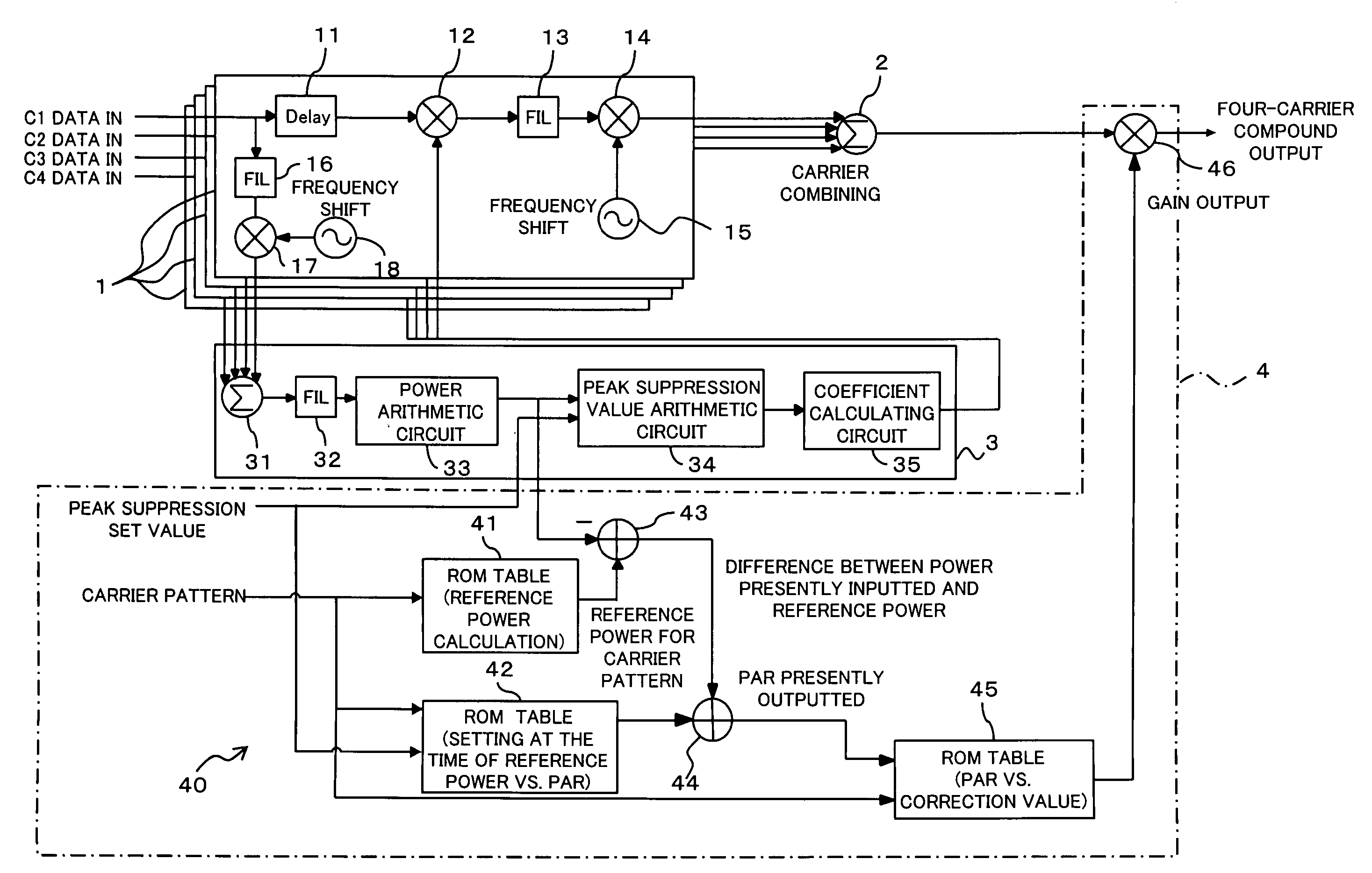
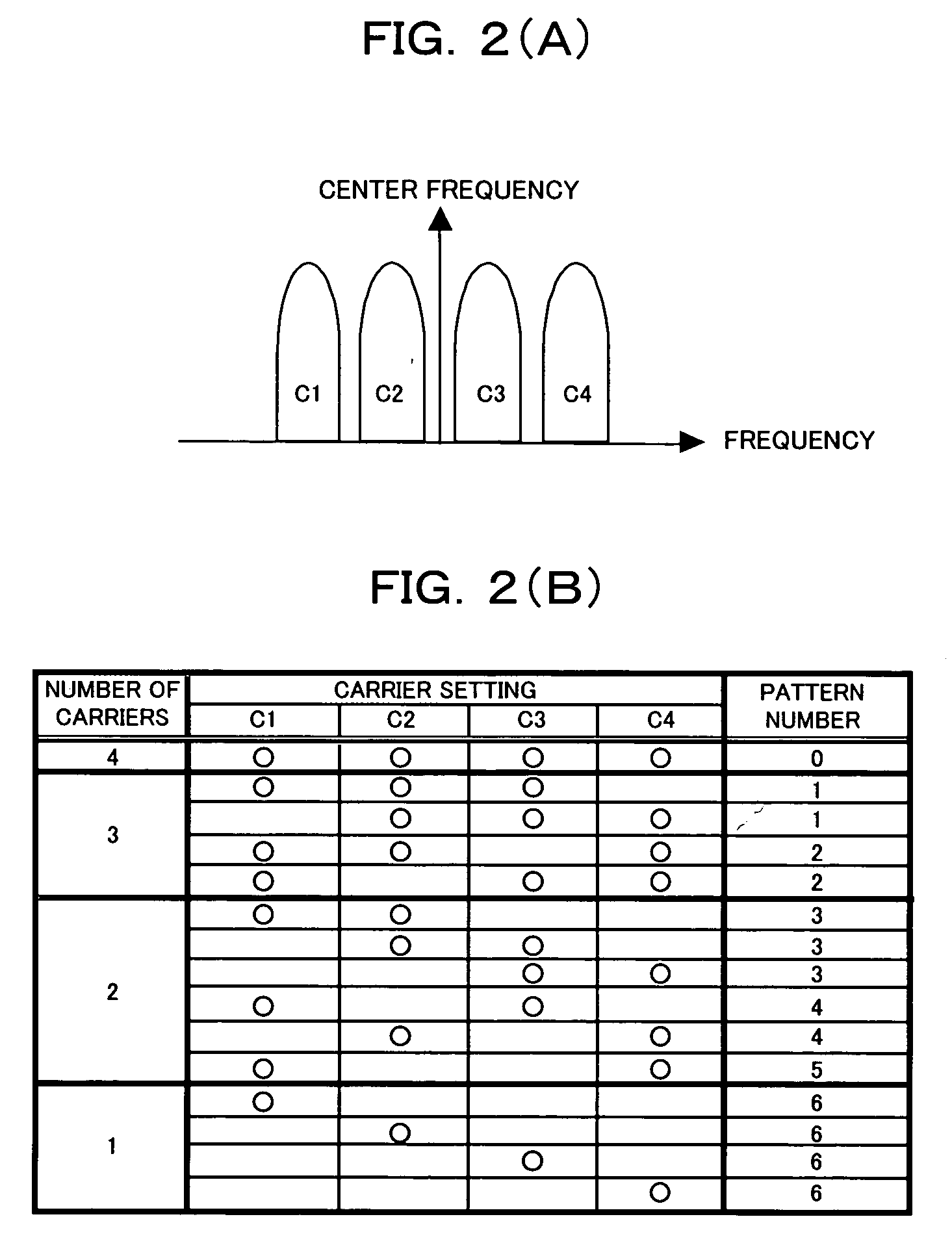
[0039]FIG. 1 is a block diagram showing structures of essential parts of a multi-carrier transmitter having an output power error absorbing circuit according to a first embodiment of the present invention. The transmitter shown in FIG. 1 comprises a carrier transmitting circuit 1 provided for each of a plurality of carrier signals (here, four carriers of C1, C2, C3 and C4), a carrier combining circuit (carrier multiplexing unit) 2 for combining (multiplexing) outputs of the carrier transmitting circuits 1, a peak suppression value arithmetic circuit (peak power suppressing unit) 3 for detecting an output peak power of the carrier combining circuits 2, correcting the gain of each carrier signal before multiplexed by the carrier combining circuit 2 according to a peak suppression setting, thereby suppressing the output peak power, and an output power error absorbing circuit 4.

[0040] Each of the carrier transmitting circuits 1 transmits a signal (car...

second embodiment

[B] Description of Second Embodiment

[0061]FIG. 8 is a block diagram showing structures of essential parts of a multi-carrier transmitter having an output power error absorbing circuit according to a second embodiment of the present invention. The transmitter shown in FIG. 8 comprises carrier transmitting circuits 1, a carrier combining circuit 2 and a peak suppressing value arithmetic circuit 3 similar to those described above with reference to FIG. 1, along with an output power error absorbing circuit 5. The internal structures of the carrier transmitting circuit 1 and the peak suppressing value arithmetic circuit 3 are identical or similar to those described above with reference to FIG. 1. In FIG. 8, like reference characters designate like or corresponding parts in FIG. 1 unless specifically mentioned.

[0062] The output power error absorbing circuit 5 detects a difference between a multiplexed (compound) power value of the carrier signals before undergone peak suppression by the ...


PUM


Abstract

A power correction value generating unit determines a power correction value for minimizing an error, from a reference output power value of a carrier multiplexed signal, generating due to peak power suppression under a carrier setting based on the carrier setting relating to either one or both of the number of carrier signals and frequency arrangement, and peak suppression setting. An output power error correcting unit corrects a signal gain before or after the carrier signals are multiplexed, using the power correction value obtained by the power correction value generating unit. In an apparatus performing peak suppression according to an input limitation power of the power amplifier, it is possible to always obtain a desirable transmission (output) power even when the number of carriers or carrier frequency arrangement varies.

Description

CROSS REFERENCE TO THE RELATED APPLICATIONS [0001] This application is based on and hereby claims priority to Japanese Application No. 2004-245113 filed on Aug. 25, 2004 in Japan, the contents of which are herby incorporated by reference. BACKGROUND OF THE INVENTION [0002] (1) Field of the Invention [0003] The present invention relates to an output power error absorbing circuit and a multi-carrier transmitter having the same, relating to a technique suitable for use to a radio communication apparatus having a multi-carrier amplifying function used in a cellular telephone system, a basic communication system, a broadcasting system or the like, for example. [0004] (2) Description of Related Art [0005] In the known code multiplexed signal circuit used in a transmitter in CDMA (Code Division Multiple Access) system, a power peak generates when codes and carrier signals are multiplexed, the peak components fall within the saturation region of the gain characteristic of the power amplifie...

Claims


Application Information

Patent Timeline
IPC IPC(8): H04B7/00H04B1/00H04Q7/20H04B1/04H04B1/707H04J13/00
CPCH04L27/2614
Inventor OHBA, TAKESHIFUNYU, YASUHITOABE, HIROAKINAKAMURA, TOMOHIRO
Owner FUJITSU LTD
Why Eureka
Try Eureka