Wire-bonding method for connecting wire-bond pads and chip and the structure formed thereby

a wire-bonding pad and chip technology, applied in the direction of electrical equipment, semiconductor devices, semiconductor/solid-state device details, etc., can solve the problems of reducing product yield and damage to the wire bonder

Inactive Publication Date: 2006-03-09
ADVANCED SEMICON ENG INC
View PDF19 Cites 34 Cited by
  • Summary
  • Abstract
  • Description
  • Claims
  • Application Information

AI Technical Summary

Benefits of technology

[0013] It is an object of the present invention to provide a wire-bonding method for connecting a wire-bond pad and a chip, and a package having a structure formed by the wire-bonding method, so as to solve the short circuit problem caused by two adjacent wire-bond pads on a substrate during a wire bonding process.

Problems solved by technology

Such an impact may cause the damage of the wire bonder and the reduction of product yield.

Method used


Image

  • Wire-bonding method for connecting wire-bond pads and chip and the structure formed thereby
  • Wire-bonding method for connecting wire-bond pads and chip and the structure formed thereby
  • Wire-bonding method for connecting wire-bond pads and chip and the structure formed thereby

Examples


Embodiment Construction

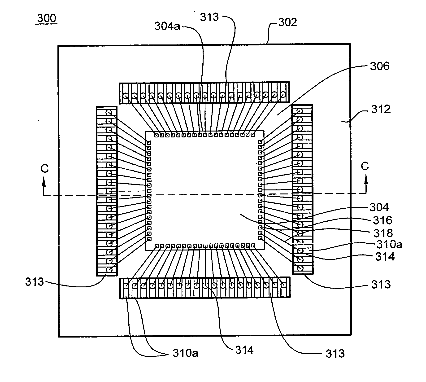
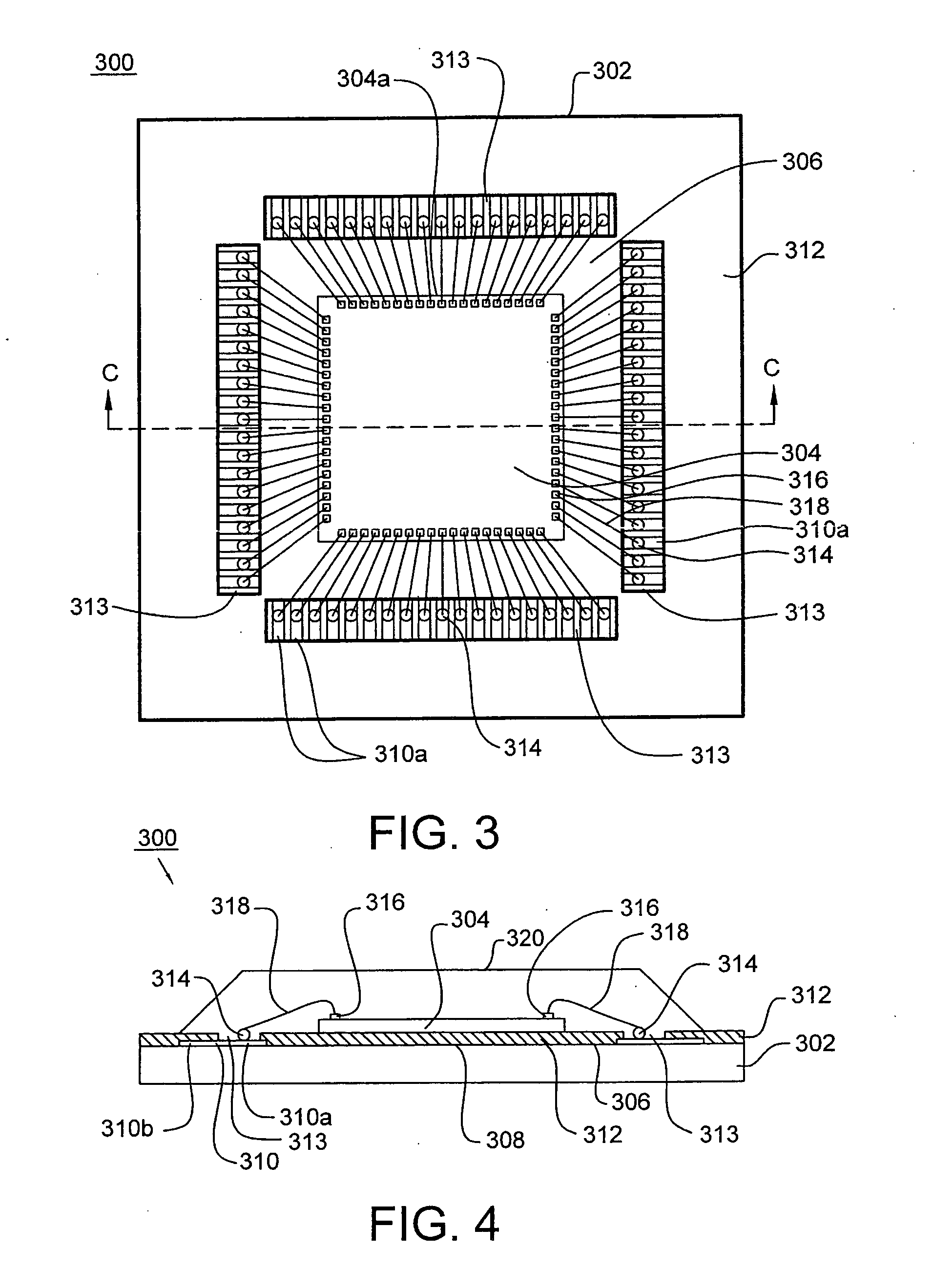
[0024]FIG. 3 shows a top plan view of a semiconductor package 300 formed by using the wire-bonding method of the present invention. FIG. 4 shows a cross-sectional view taken along line C-C of FIG. 3.

[0025] Referring to FIGS. 3 and 4, the semiconductor package 300 includes a substrate 302 and a semiconductor chip 304 disposed on the substrate 302. The substrate 302 has an upper surface 306 and a chip area 308 defined on the upper surface 306 for supporting the semiconductor chip 304. The substrate 302 further includes a plurality of conductive traces 310 formed on the upper surface 306, wherein each of the conductive traces 310 has a section 310a, also referred to as a wire-bond pad, and a terminal part 310b. The sections 310a are arranged side by side around the chip area 308, and the terminal parts 310b are used for being electrically connected to other circuit contacts. A solder mask 312 covers the conductive traces 310 with the sections 310a exposed therefrom. In this embodiment...


PUM


Abstract

A wire-bonding method for connecting a wire-bond pad and a chip is characterized in that a metal ball is disposed on the wire-bond pad such that a bonding wire can be electrically connected to the wire-bond pad and raised to a certain height by the metal ball. In this arrangement, the short circuit problem caused by two adjacent wire-bond pads and impact problem on a solder mask caused by a bond head of a wire bonder during a wire bonding process can be avoided. The present invention also provides a package having a structure formed by the above-mentioned wire-bonding method.

Description

CROSS REFERENCE TO RELATED APPLICATION [0001] This application claims the priority benefit of Taiwan Patent Application Serial Number 093127001, filed on Sep. 7, 2004, the full disclosure of which is incorporated herein by reference. BACKGROUND OF THE INVENTION [0002] 1. Field of the Invention [0003] The present invention generally relates to a wire-bonding method, and more particularly to a wire-bonding method for connecting a wire-bond pad and a chip. [0004] 2. Description of the Related Art [0005] In the semiconductor packaging process, a semiconductor chip is electrically connected to a packaging substrate or a lead frame through a bonding technique such as the wire bonding, the tape automatic bonding (TAB), or the flip-chip bonding technique. Even though the wire bonding technique is the earliest one to be used as compared with the tape automatic bonding (TAB) and the flip-chip bonding techniques, it is still presently and widely used due to the advantages of simply and easily ...

Claims


Application Information

Patent Timeline
Patent Type & Authority Applications(United States)
IPC IPC(8): H01L23/48
CPCH01L23/49811H01L2924/00014H01L2224/48091H01L2224/48228H01L2224/48475H01L2224/4848H01L2224/49171H01L2224/85051H01L2224/92H01L2224/92247H01L2924/01028H01L2924/0105H01L2924/01079H01L2924/01082H01L2224/48227H01L2924/014H01L2924/01006H01L2924/01005H01L24/48H01L24/49H01L24/85H01L2224/78H01L2924/00H01L2224/05554H01L2924/181H01L2224/45099H01L2224/05599H01L2224/48465H01L2924/00012
Inventor LIN, YI MIN
Owner ADVANCED SEMICON ENG INC
Why Eureka
Try Eureka