Package apparatus and manufacturing method thereof

a packaging apparatus and manufacturing method technology, applied in the direction of electrical apparatus, semiconductor devices, semiconductor/solid-state device details, etc., can solve the problems of high cost, troublesome wiring, repeating,

Active Publication Date: 2016-06-09
PHOENIX PIONEER TECH
View PDF6 Cites 2 Cited by
  • Summary
  • Abstract
  • Description
  • Claims
  • Application Information

AI Technical Summary

Problems solved by technology

However, the aforesaid conventional fiberglass substrate packaging structure is very costly for using a fiberglass substrate as its substrate and the thin-type fiberglass substrate can be easily deformed and wrapped.
The conventional substrate including fiberglass will increase the difficulty of processing for laser via so that it cannot fit the need of fine pitch, and therefore make the wiring more troublesome; and as the blind / buried vias in the aforesaid multi-layered metal laminated structure are formed by the repetition of a laser via method, such repetition can be a complex and time consuming process.
Since the electrical connections between the plural bonding structures in the package structure are achieved through the TMV whereas such TMV should be fabricated by the use of a laser via process, the whole package fabrication process can be very costly.

Method used


Image

  • Package apparatus and manufacturing method thereof
  • Package apparatus and manufacturing method thereof
  • Package apparatus and manufacturing method thereof

Examples


first embodiment

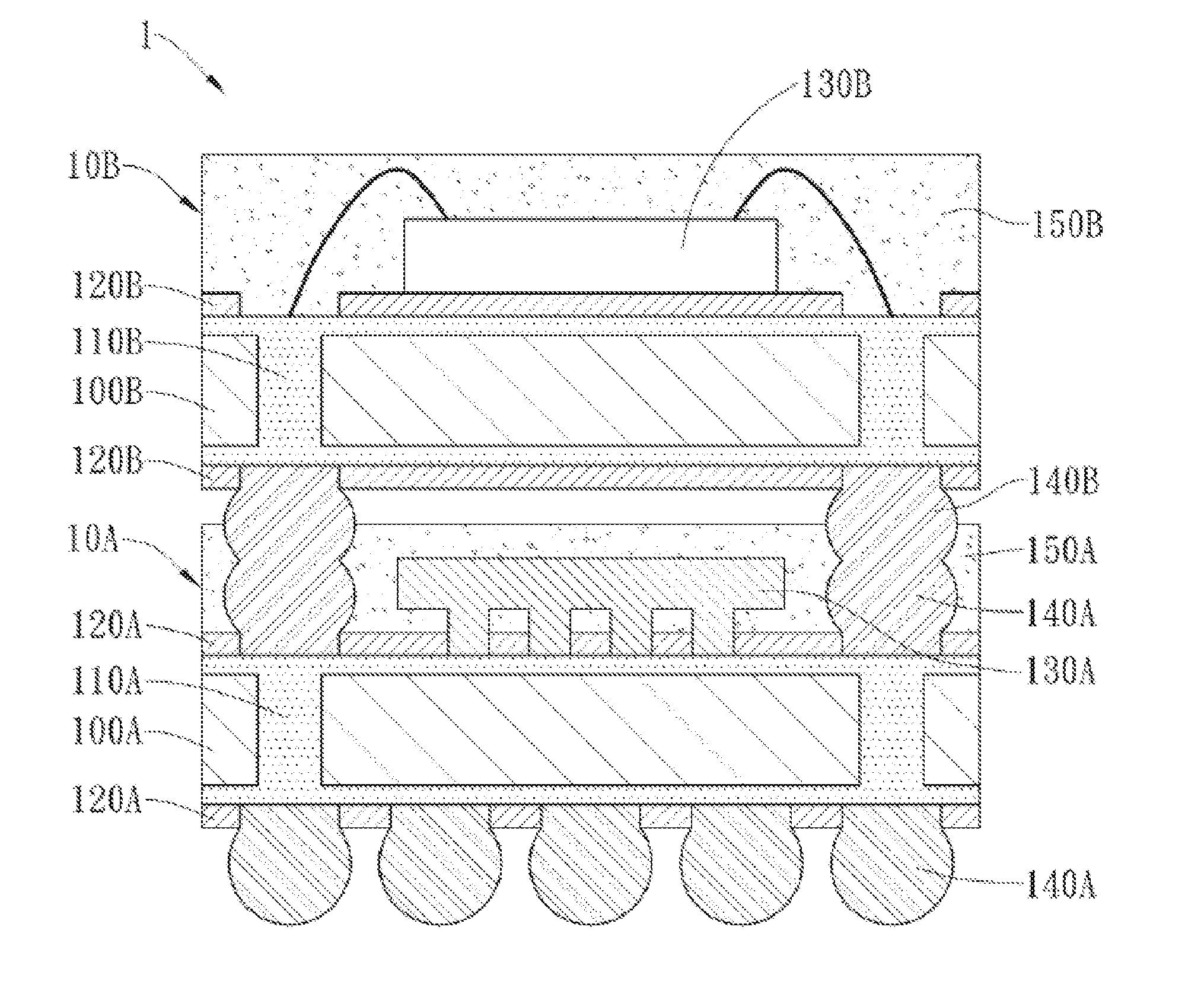
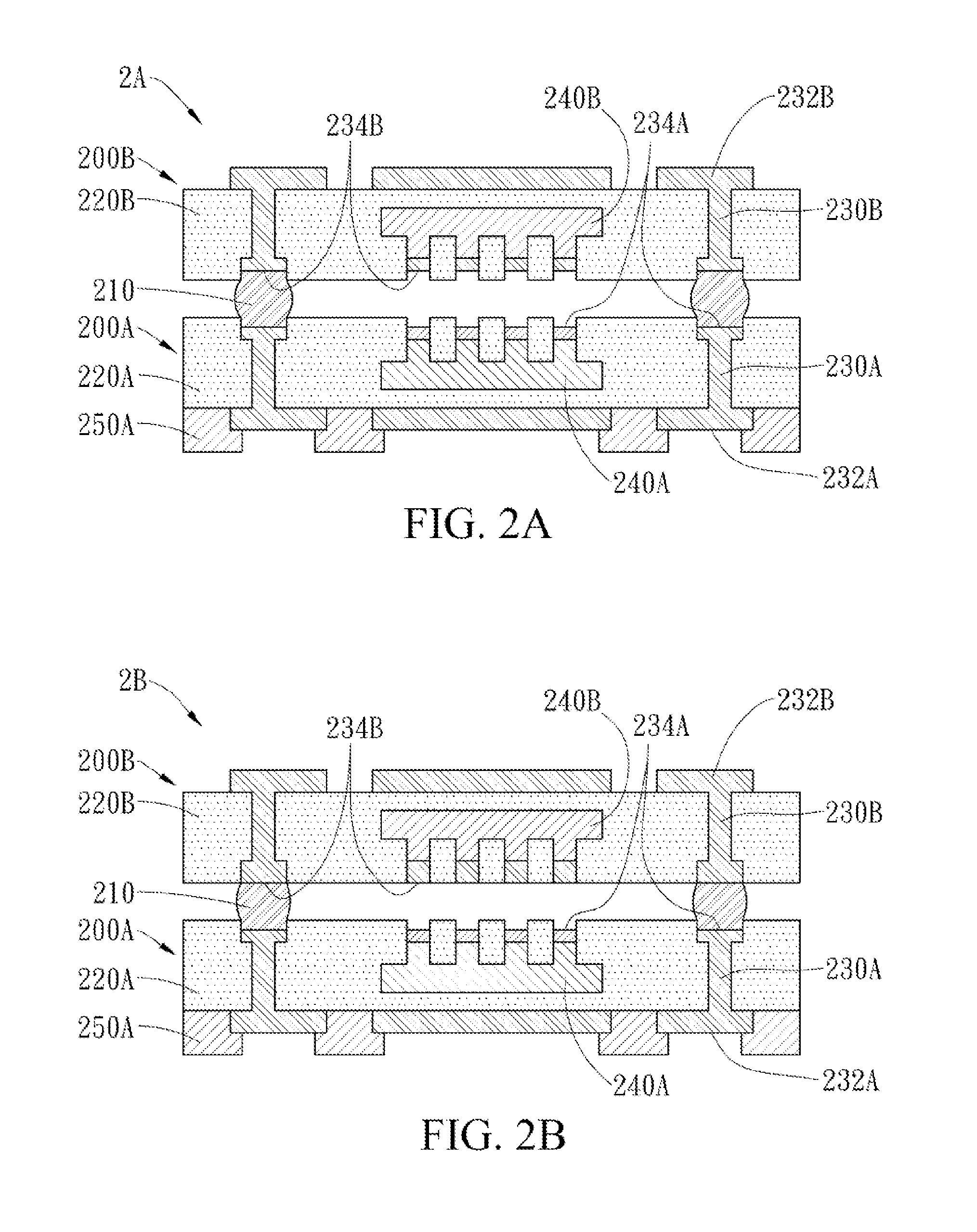
[0077]Please refer to FIG. 2A, which is a schematic diagram showing a package apparatus according to the present invention. In FIG. 2A, a package apparatus 2A is disclosed, which comprises: a first package module 200A, a second package module 200B and a plurality of conductive elements 210. The first package module 200A comprises: a first molding compound layer 220A, a first conductive pillar layer 230A, a first internal component 240A, and a first protection layer 250A. The first conductive pillar layer 230A is formed with a first surface 232A and a second surface 234A that are arranged opposite to each other while being disposed in the first molding compound layer 220A. The first internal component 240A is electrical connected to the first conductive pillar layer 230A and disposed in the first molding compound layer 220A. The first protection layer 250A is disposed on the first molding compound layer 220A and the first surface 232A of the first conductive pillar layer 230A.

[0078]S...

third embodiment

[0095]Please refer to FIG. 5B to FIG. 5F, which are schematic diagrams respectively showing a package apparatus according to a twentieth embodiment to a twenty-third embodiment of the present invention. Each of the package apparatuses 5B to 5F of these embodiments is structured similar to the package apparatus 5A of the nineteenth embodiment, but is different in that: in the package apparatus 5B, the second surface 234B of the second conductive pillar layer 230B is positioned coplanar with the second molding compound layer 220B; in the package apparatus 5C, the second surface 234B of the second conductive pillar layer 230B is higher than the second molding compound layer 220B; in the package apparatus 5D, the second molding compound layer 220B is formed covering all the lateral surface of the second surface 234B of the second conductive pillar layer 230B, despite that the second surface 234B of the second conductive pillar layer 230B is lower than the second molding compound layer 2...

sixth embodiment

[0123]Please refer to FIG. 17A, which is a schematic diagram showing a package apparatus according to a seventieth embodiment of the present invention. The package apparatus 17A of this seventieth embodiment is structured similar to the package apparatus 12A of the fortieth embodiment, but is different in that: in the package apparatus 17A, the second surface 234A of the first conductive pillar layer 230A is higher than the first molding compound layer 220A while allowing the first molding compound layer 220A to be formed covering all the lateral surface of the second surface 234A of the first conductive pillar layer 230A, despite that the second surface 234B of the second conductive pillar layer 230B is still lower than the second molding compound layer 220B. Moreover, the apparatus shown in this forty-sixth embodiment can be varied in many ways similar to those aforesaid embodiments, such as the second surface 234B of the second conductive pillar layer 230B can be positioned copla...


PUM


Abstract

A package apparatus includes a first package module, a second package module and multiple conductive elements. The first package module includes a first molding compound layer, a first conductive pillar layer disposed in the first molding compound layer, a first internal component, and a first protection layer. The first internal component electrically connects to the first conductive pillar layer and disposed in the first molding compound layer. The first protection layer is disposed on the first molding compound layer and the first conductive pillar layer. The second package module includes a second molding compound layer, a second conductive pillar layer disposed in the second molding compound layer, and a second internal component. The second internal component electrically connects to the second conductive pillar layer and disposed in the second molding compound layer. The conductive elements are disposed between the first and the second conductive pillar layers.

Description

FIELD OF THE INVENTION[0001]The present invention relates to a package apparatus and manufacturing method thereof, and more particularly, to a semiconductor package apparatus and method for manufacturing the same.BACKGROUND OF THE INVENTION[0002]With the design trend in electronic devices is toward lighter, smaller, thinner but more functional devices with performance requirements continuing to increase, device manufacturers increasingly need specialty integrated circuit (IC) solutions for allowing billions of miniature electronic components to be densely packed in a small area. Thus, device manufacturers come up with innovative packaging techniques for embedding electronic components in a substrate while allowing shorter traces between the electronic components and the substrate. In addition, the layout area is increased by the use of built-up technique as the technology advances for achieving lighter, smaller, thinner and more functional high-performance devices.[0003]Generally, m...

Claims


Application Information

Patent Timeline
Patent Type & Authority Applications(United States)
IPC IPC(8): H01L25/065H01L23/29H01L23/498H01L23/00H01L25/00H01L23/31
CPCH01L25/0657H01L25/50H01L23/3114H01L23/49827H01L24/48H01L24/16H01L2225/0652H01L2225/0651H01L2225/06517H01L2225/06548H01L2225/06572H01L2224/16227H01L2224/48227H01L23/293H01L2224/48091H01L23/3107H01L23/49811H01L23/5389H01L25/105H01L25/117H01L2225/1023H01L2225/1035H01L2225/1058H01L2924/00014H01L2924/181H01L2924/00012H01L2224/45099H01L2224/45015H01L2924/207H01L23/4012H01L25/043H01L25/0756
Inventor HU, CHU-CHINHSU, SHIH-PINGCHOU, E-TUNG
Owner PHOENIX PIONEER TECH
Why Eureka
Try Eureka