Switching circuit

a technology of switching circuit and current wave, which is applied in the direction of pulse technique, process and machine control, instruments, etc., can solve the problems of difficulty in amplifying current wave up to high frequency and maintaining high gain capacity, and achieve low cost, high speed, and low impedance

Inactive Publication Date: 2006-03-09
SHINDENGEN ELECTRIC MFG CO LTD
View PDF6 Cites 0 Cited by
  • Summary
  • Abstract
  • Description
  • Claims
  • Application Information

AI Technical Summary

Benefits of technology

[0006] In view of the above problem, the present invention is to provide a switching circuit with a low cost having a current detecting circuit that detects current waveform of the main switch in form of a real time waveform in high speed and outputs it in form of a large signal with low impedance.
[0007] In the present invention, the above-described object is achieved by providing the current detecting circuit that can output large current waveform while keeping difference of input voltage of an amplifier to be about zero volt. And by connecting the third switch, of which gate signal synchronizes that of the main switch, between a first resistance element and a subsidiary switch, voltage waveform of the second resistance element becomes similar to that of current waveform of the main switch, so that the current waveform with a high speed can be treated as a large voltage signal.
[0008] When the first resistance element made from poly-silicon resistance is formed on an insulating film, insulation between the main switch and the first resistance element can be formed easily and a highly integrated circuit may be possible and parasitic capacity etc. becomes small so that high speed operation becomes possible. When the first resistance element is formed so as to have its temperature coefficient with higher positive value than that of the main switch, in the current detecting circuit using the first resistance element, it is possible to easily provide a switching circuit with stronger function of anti-heat-bursting. Therefore, a current detecting circuit with many excellent features can be easily formed.

Problems solved by technology

Because current waveform includes components of high frequency, it was actually difficult to amplify the current wave up to high frequency keeping a high gain capacity.

Method used


Image

  • Switching circuit
  • Switching circuit
  • Switching circuit

Examples


embodiment 1

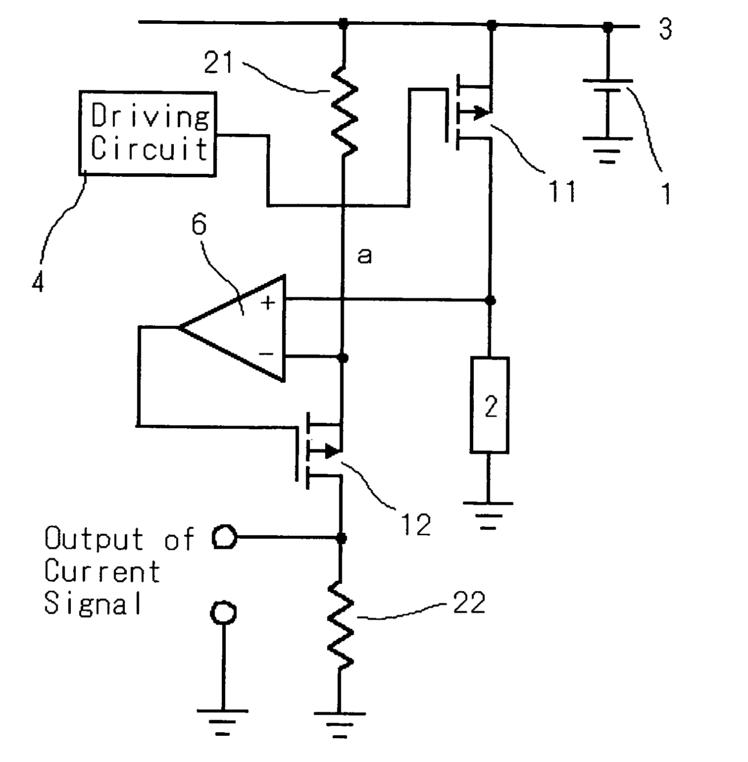
[0032] The first embodiment of the switching circuit according to the present invention is shown in FIG. 1. 1 is an input power source, 2 is a load, 3 is fixed potential, 4 is a driving circuit, 6 is an amplifier, 11 is a main switch, 12 is a subsidiary switch, 13 is a third switch, 14 is a current detecting switch, 15 is a high side switch, 21 is a first resistance element, and 22 is a second resistance element.

[0033] The switching circuit according to the present embodiment comprises a main switch 11 composed of p-channel MOSFET, whose on-voltage shows resistance characteristics wherein a gate terminal of the main switch 11 is connected to a driving circuit 4. And a source terminal of the main switch is connected to the fixed potential 3 and a drain terminal thereof is connected to the load circuit 2. In addition, the fixed potential 3 may be connected to the drain terminal of the main switch 11 and the load circuit 2 may be connected to the source terminal of the main switch 11....

embodiment 2

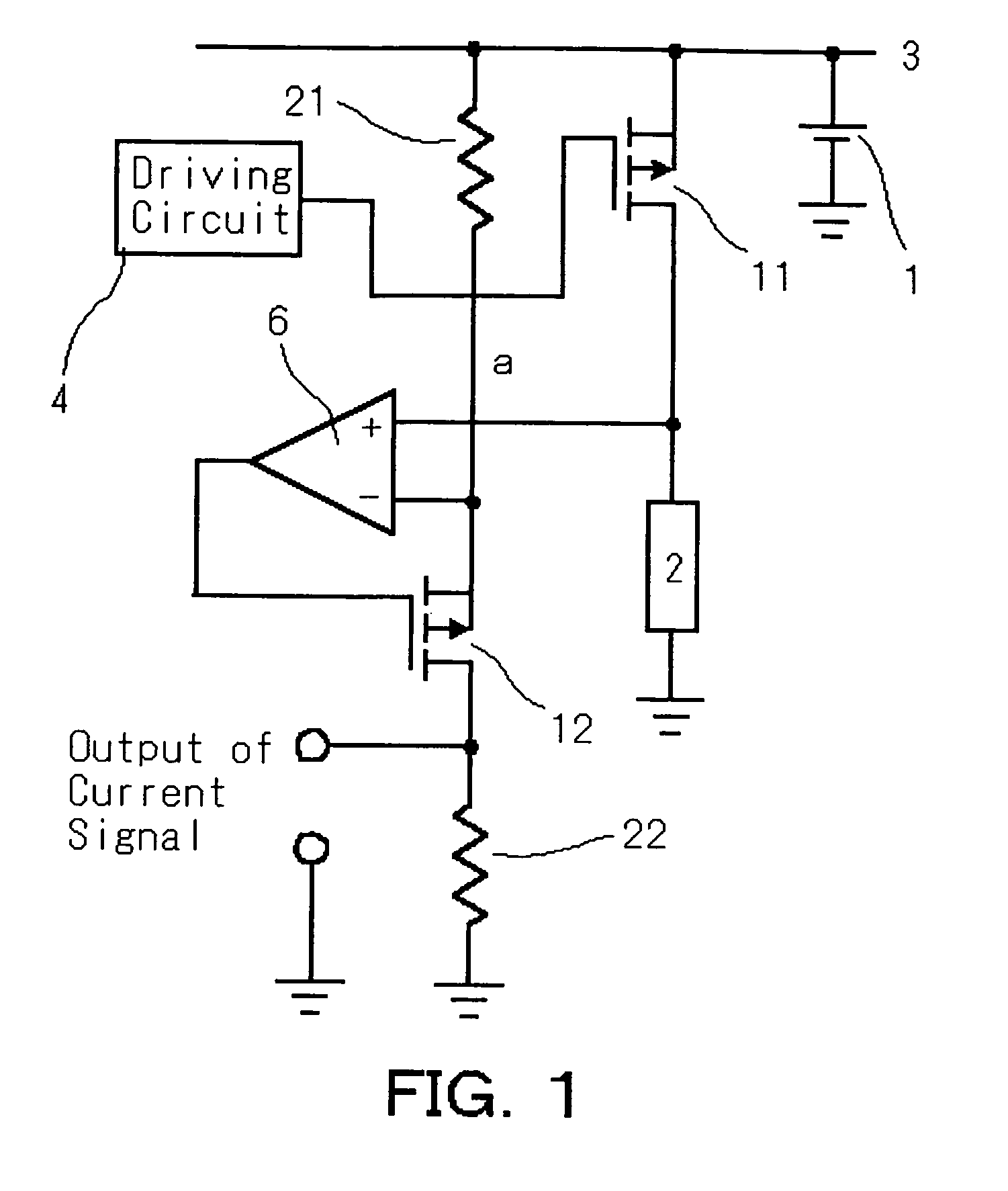
[0036] The second embodiment is shown in FIG. 2. This embodiment is almost the same as that of the first embodiment. This embodiment is characterized in that the main switch 11 is composed of n-channel MOSFET. Detection of current can be also conducted by the same way as that of the first embodiment. However, polarity characteristics of output voltage of the driving circuit 4 is different from that of the first embodiment, that is, in the first embodiment, the main switch 11 becomes conductive by negative gate potential to the source potential, on the other hand, the main switch 11 becomes conductive by positive gate potential to the source potential in the case of this embodiment.

embodiment 3

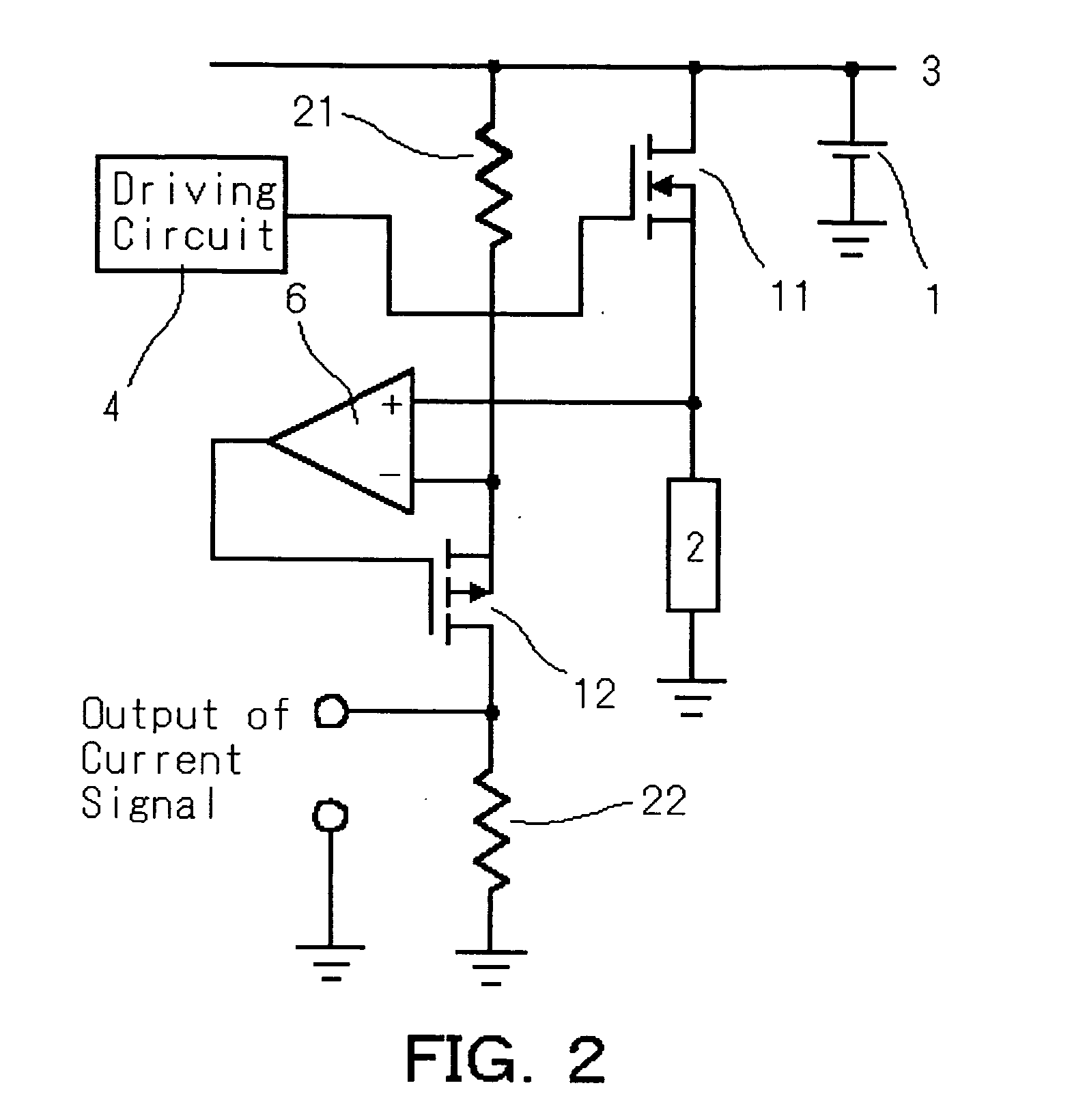
[0037] The third embodiment is shown in FIG. 3. In this embodiment, the first resistance element 21 is connected to a source terminal of the third switch 13, wherein a drain terminal is connected to the source terminal of the subsidiary switch 12. And the gate terminal of the third switch 13 is connected to the driving circuit 4 and the gate signal of the third switch 13 is so constructed as to synchronize with that of the gate signal of the main switch 11. That is, since the main switch 11 is p-channel MOSFET in this embodiment, the third switch 13 is also p-channel MOSFET.

[0038] Because in the case of the third embodiment, the gate signal of the main switch 11 is so constructed as to synchronize with that of the gate signal of the third switch 13, when the main switch 11 is on off-state, and the third switch 13 is also on off-state, it is possible to prevent large current from flowing through the first resistance element 21. Therefore, a current detecting circuit with electric po...


PUM


Abstract

The present invention provides a switching circuit comprising a current detecting circuit that detects current waveform of a main switch in real time waveform and outputs it in low impedance. The switching circuit comprises the current detecting circuit having the main switch (11), of which on-voltage shows resistance characteristics, wherein a gate terminal is connected to a driving circuit (4) and further either terminal of drain or source thereof is connected to a fixed potential (3) and the other terminal thereof is connected to a load circuit (2) respectively, a first resistance element (21), of which resistance value is higher than on-resistance of the main switch connected to the fixed potential (3), a subsidiary switch (12), a source terminal thereof is connected to the first resistance element (21), an amplifier (6) that amplifies comparatively voltage generated in the first resistance element (21) and outputs to a gate terminal of the subsidiary switch (12) and the second resistance element (22) that generates voltage by amplifying on-current of the main switch (11) by connecting to the drain terminal of the subsidiary switch (11).

Description

FIELD OF THE INVENTION [0001] The present invention relates to a circuit for detecting current of a switch by detecting on-voltage of a power switch. RELATED ART [0002] A first conventional example of a switching circuit having a current detecting circuit is shown in FIG. 10. This conventional example is equipped with a main switch 111 composed of MOSFET, of which on-voltage shows resistance characteristics, and a gate terminal of the main switch 111 is connected to a driving circuit 104. And a drain terminal of the main switch 111 is connected to a fixed potential 103, and a source terminal thereof is connected to a load circuit 102. A current detecting circuit installed in the switching circuit has a current detecting switch 114 wherein a drain terminal thereof is connected to the fixed potential and a gate terminal thereof is connected to the driving circuit 104. Further, a source terminal of the current detecting switch 114 is connected to a resistance element 121 and a positive...

Claims


Application Information

Patent Timeline
Patent Type & Authority Applications(United States)
IPC IPC(8): G05F1/10H03K17/082
CPCH03K17/0822H03K17/08H03K17/687
Inventor KUBOTA, KENICHIOHSHIMA, MASAKINOZAKI, YUKIHIROHAGA, HIROYUKI
Owner SHINDENGEN ELECTRIC MFG CO LTD
Why Eureka
Try Eureka