Liquid crystal display device and driving method thereof

a technology of liquid crystal display and driving method, which is applied in the direction of instruments, static indicating devices, etc., can solve the problems of increased afterimage, increased cost, and increased cost of scanning line drive circuit, and achieve the effect of preventing additional cos

Inactive Publication Date: 2006-03-09
MITSUBISHI ELECTRIC CORP
View PDF13 Cites 37 Cited by
  • Summary
  • Abstract
  • Description
  • Claims
  • Application Information

AI Technical Summary

Benefits of technology

[0013] The liquid crystal display device is capable of producing a scanning line signal including two pulses of the phase shifted fist and second signals without employing a particular circuit structure. It is therefore unnecessary to use a particular gate array and the like, thereby preventing additional cost.

Problems solved by technology

When the impulse-type display device is compared with the hold-type display device, the hold-type had a problem of causing a more conspicuous afterimage when displaying a moving image.
This requires a gate array and so on that are different from those in the common liquid crystal display device, which incurs additional cost.
In addition, when forming the liquid crystal display device of JP 2004-041002 in which a signal divided into an image signal portion and a black signal portion within a horizontal scanning period is supplied to a pixel, a scanning line signal (first signal) for writing an image signal and a scanning line signal (second signal) for writing a black signal are phase shifted to one another, and therefore cannot be produced by a scanning line drive circuit formed by a simple shift register.
For this reason, it is required in JP 2004-041002 that a scanning line drive circuit having a different structure from the conventional ones be employed, which incurs additional cost.

Method used


Image

  • Liquid crystal display device and driving method thereof
  • Liquid crystal display device and driving method thereof
  • Liquid crystal display device and driving method thereof

Examples


first preferred embodiment

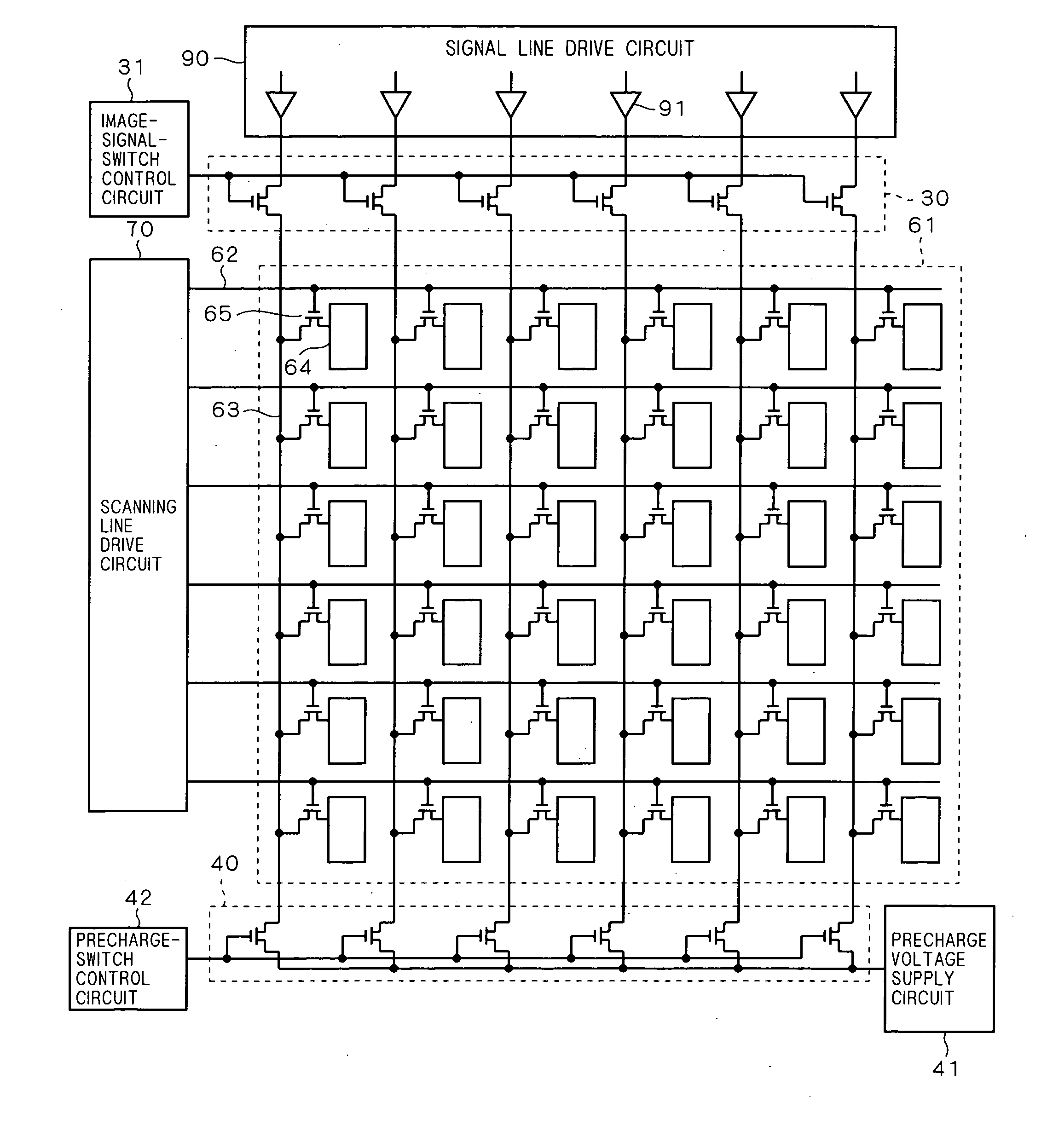
[0031] First, FIG. 14 shows the structure of a liquid crystal display device in which a signal supplied to a pixel is divided into an image signal portion and a black signal portion within a horizontal scanning period. A liquid crystal display device 1 shown in FIG. 14 includes a gate array 10, a movement determination processing part 20, and a liquid crystal module 60. The liquid crystal module 60 includes a liquid crystal panel 61, a scanning line drive circuit 70, and a signal line drive circuit 90. Further, the liquid crystal panel 61 includes a plurality of scanning lines 62, a plurality of signal lines 63 that cross the scanning lines 62, pixels 64 arranged in a matrix, and TFTs (Thin Film Transistor) 65 provided correspondingly to the pixels 64.

[0032] Each of the TFTs 65 has a gate electrode connected to the scanning line 62, a source electrode connected to the signal line 63, and a drain electrode connected to the pixel 64. Consequently, by controlling the voltage of the sc...

second preferred embodiment

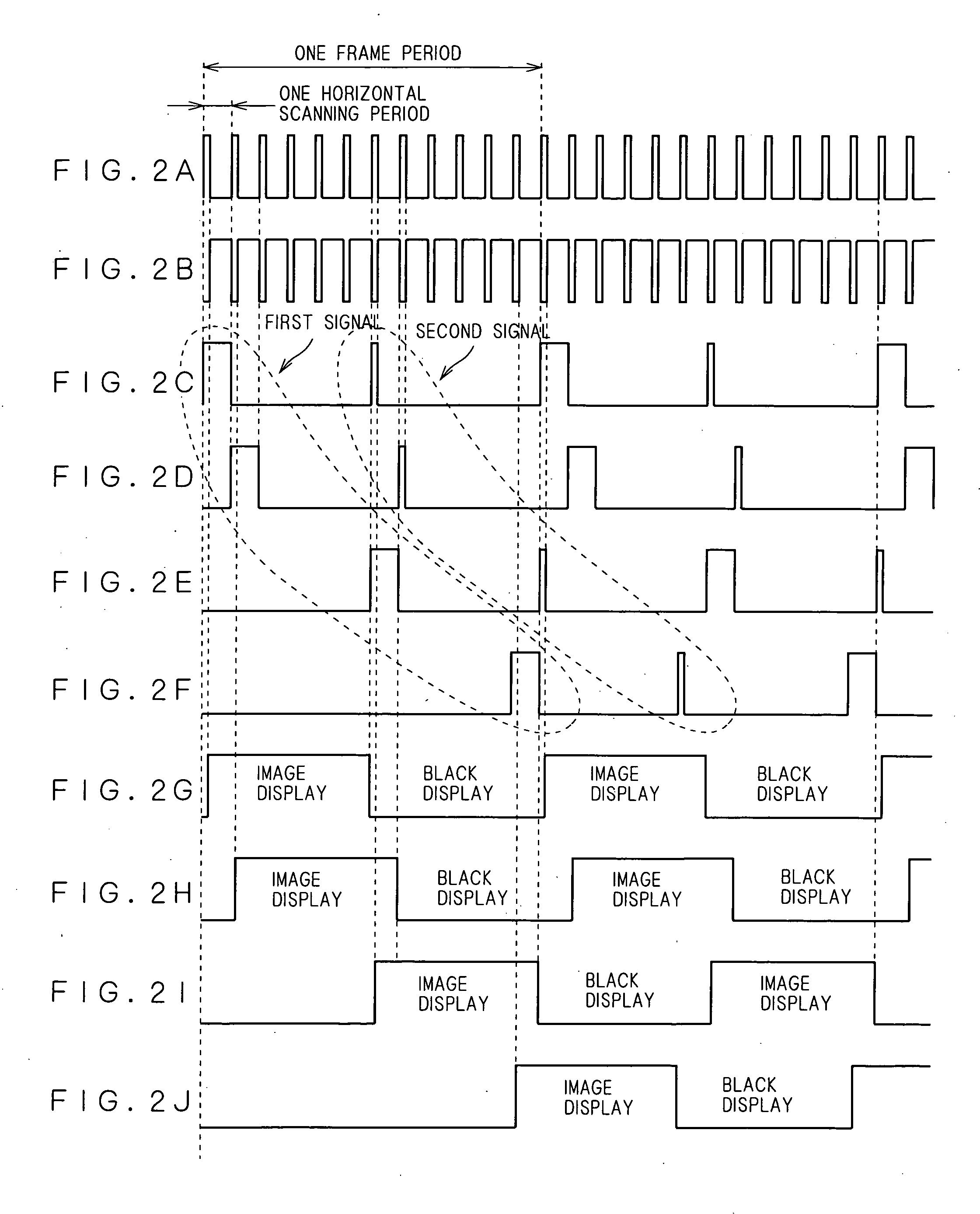
[0055] In a second preferred embodiment of the present invention, the structure of the scanning line drive circuit 70 in the liquid crystal display device according to the first preferred embodiment will be specifically described. The scanning line drive circuit 70 according to this embodiment outputs two scanning line signals (first signal and second signal) having a pulse width of the horizontal scanning period and a pulse width of the precharge period, respectively, by using two shift registers.

[0056]FIG. 3 shows the structure of the scanning line drive circuit 70 according to this embodiment. This scanning line drive circuit 70 includes a first shift register 71 latched at the timing of a vertical synchronizing signal STV. The first shift register 71 includes as many flip-flop circuits as the scanning lines 62, and produces the first signal of the scanning line signal to be supplied to the respective scanning lines 62. The scanning line drive circuit 70 shown in FIG. 3 further ...

third preferred embodiment

[0064] In a third preferred embodiment of the present invention, the second shift register 72 is omitted in the scanning line drive circuit 70 according to the second preferred embodiment by fixing the settings of the counter 73 to half the number of scanning lines.

[0065]FIG. 6 shows the structure of the scanning line drive circuit 70 according to this embodiment. In this scanning line drive circuit 70, the counter 73 outputs a timing signal shifted by horizontal scanning periods in accordance with half the total number of scanning lines with reference to the vertical synchronizing signal STV. A flip-flop circuit 78 is supplied with the vertical synchronizing signal STV and the timing signal from the counter 73, and outputs a signal (hereafter called an FF signal) that is switched between a high state and a low state within half a frame period and its inversion signal (hereafter called an FF inversion signal).

[0066] The first shift register 71 is supplied with the vertical synchro...


PUM


Abstract

A liquid crystal display device includes a pixel, an image signal switch connected to a signal line and a signal line drive circuit, a precharge switch connected to a scanning line and a precharge voltage supply circuit, and a scanning line drive circuit supplying successively a scanning line signal including a first signal and a second signal within one frame period to the scanning line in each row. The image signal switch is turned on while the first signal is supplied from the scanning line drive circuit, whereby an image signal is written into the pixels, and only the precharge switch is turned on while the second signal is supplied from the scanning line drive circuit, whereby a precharge voltage is written into the pixels.

Description

BACKGROUND OF THE INVENTION [0001] 1. Field of the Invention [0002] The present invention relates to liquid crystal display devices and driving methods thereof, and especially to liquid crystal display devices displaying mainly moving images and driving methods thereof. [0003] 2. Description of the Background Art [0004] Conventional image display devices are roughly divided into two types: an impulse-type display device (e.g. CRT) that displays an image for a sufficiently short period of time with respect to a fame period, and a hold-type display device (e.g. liquid crystal display device) that keeps holding an image display of a previous frame until a new image is written. [0005] When the impulse-type display device is compared with the hold-type display device, the hold-type had a problem of causing a more conspicuous afterimage when displaying a moving image. This is due to pursuit movement of an eyeball and summation effects. That is, an eyeball moves successively through the pu...

Claims


Application Information

Patent Timeline
Patent Type & Authority Applications(United States)
IPC IPC(8): G09G3/36
CPCG09G3/3648G09G3/3677G09G2320/106G09G2310/06G09G2320/0261G09G2310/0248G09G3/36G09G3/20
Inventor KAWAGOE, HISASHI
Owner MITSUBISHI ELECTRIC CORP
Why Eureka
Try Eureka