System and method for preparing micro-nano array structure by means of laser light

A technology of array structure and micro-lens array, which is used in laser welding equipment, welding equipment, manufacturing tools, etc., can solve the problem of uneven plane distribution of energy beam spots, inability to process hundreds of micro-nano structures in parallel, and high spot center energy. Problems such as low edge energy

Active Publication Date: 2015-03-25
TECHNICAL INST OF PHYSICS & CHEMISTRY - CHINESE ACAD OF SCI
View PDF11 Cites 25 Cited by
  • Summary
  • Abstract
  • Description
  • Claims
  • Application Information

AI Technical Summary

Problems solved by technology

[0005] However, the above-mentioned processing method has the following disadvantages: because the laser beam spot has a Gaussian energy distribution, the center energy of the spot is high and the edge energy is low, and the energy beam spot is unevenly distributed in the plane
However, compared with microlens array processing, this method cannot process hundreds of micro-nano structures in parallel at the same time, and cannot realize the preparation of large-area, arrayed structures.

Method used


Image

  • System and method for preparing micro-nano array structure by means of laser light
  • System and method for preparing micro-nano array structure by means of laser light
  • System and method for preparing micro-nano array structure by means of laser light

Examples


Embodiment 1

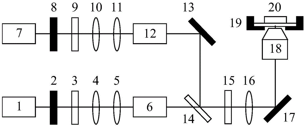
[0121] The following combination Figure 7 with Figure 8 The present invention will be described in detail by taking the preparation of a silver nano-dot array with a single beam on a glass substrate as an example.

[0122] First, the shutters 2 and 8 of the first light path and the second light path are closed, and the sample carrying the silver ion solution is placed on the micro moving stage.

[0123] The sample carrying the silver ion solution includes a glass substrate to be processed, a silver ion solution applied on the substrate, and a transparent auxiliary substrate. The concentration of silver ions in the silver ion solution is 0.01M-0.5M, and the concentration of the surfactant n-decylphthalein sarcosine sodium salt is 0.01M-0.2M. In order to prevent the evaporation of the solution during the manufacturing process of the metal micro / nano structure, a sandwich structure consisting of a glass substrate to be processed, a silver ion solution and a transparent auxiliary sub...

Embodiment 2

[0136] The following combination Figure 7 with Picture 9 The present invention will be described in detail by taking the preparation of a silver nanowire array on a glass substrate with a single beam as an example.

[0137] Keep the other conditions the same as in Example 1. Adjust the total power of the femtosecond pulsed laser beam generated by the laser to 0.1-2.8W by adjusting the first optical attenuator located on the optical path. The moving speed of the three-dimensional micro moving stage is 20nm / ms-1nm / ms, and silver nanowire arrays with a diameter of 100-500nm can be obtained on a glass substrate.

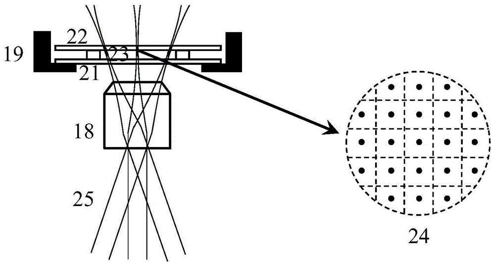
[0138] Picture 10 In order to use the method of producing metal nanowires using laser light of the present invention, a microlens array with a period of 600 microns splits the flat-top light into approximately 70 beams. Under the laser light source 780nm femtosecond laser and a 100x objective lens, the total power is 193mW, adjust 70 laser beams to focus on the interface ...


PUM

PropertyMeasurementUnit
diameteraaaaaaaaaa
diameteraaaaaaaaaa
diameteraaaaaaaaaa

Abstract

The invention discloses a system and method for preparing a micro-nano array structure by means of laser light. The method for preparing the micro-nano array structure by means of laser light comprises the steps that a first laser beam with the wavelength enabling a material to be processed to generate the multiphoton absorption effect is provided; homogenization treatment is conducted on the first laser beam in Gaussian distribution, so that a first flat beam with energy evenly distributed is obtained; the first flat beam is split into multiple laser beams arranged in an array mode by means of a microlens array component; the multiple laser beams arranged in the array mode are focused to beam focusing components located on the same plane respectively; a metal ion solution placed on a minitype movable table controlled by a computer is scanned, so that hundreds of micro-nano periodical array structures are obtained, wherein the beam spot area of the first flat beam is equal to or smaller than the effective array area of the microlens array component. According to the method for preparing the micro-nano array structure by means of laser light, the micro-nano array structures of the same structure and in controllable dimensions can be prepared in a large-scale mode rapidly.

Description

Technical field [0001] The invention relates to the field of preparation of micro-nano structures based on functional materials such as metals, polymers, composite materials and the like. More specifically, it relates to a system and method for fabricating periodic micro-nano array structures using femtosecond lasers. Background technique [0002] Because the micro-nano structure of functional materials such as metal, polymer, composite material has novel optical, electrical, and magnetic properties, it is used in micro-nano optoelectronic devices, surface plasmon resonance and transmission, high-sensitivity chemical and biological sensors, high Integrated photoelectric devices, solar cell three-dimensional nano-electrodes and artificial metamaterials have important application potential. Therefore, research on the preparation methods of functional materials micro-nano structures has also received extensive attention. [0003] At present, femtosecond laser multiphoton reduction is...

Claims


Application Information

Patent Timeline
Patent Type & Authority Applications(China)
IPC IPC(8): B23K26/06
CPCB23K26/0643B23K26/0648B23K26/352
Inventor 段宣明赵圆圆郑美玲赵震声
Owner TECHNICAL INST OF PHYSICS & CHEMISTRY - CHINESE ACAD OF SCI
Why Eureka
Try Eureka