Projection exposure apparatus and method for producing a printed circuit board

a technology of projection exposure and printed circuit board, which is applied in the direction of circuit masks, printers, instruments, etc., can solve the problems of only exposing the plurality of patterns on the board, and the stepper method cannot expose so far such coupons

Active Publication Date: 2006-03-09
ADTEC ENG
View PDF9 Cites 5 Cited by
  • Summary
  • Abstract
  • Description
  • Claims
  • Application Information

AI Technical Summary

Benefits of technology

[0015] A masking device may be used for masking other area than the certain area of the photo mask in order to defin...

Problems solved by technology

With such a large-sized board, it is impossible to expose the circuits at one time because the size of the board is larger than the irradiation area of an exposing light source.
However, the stepper method can expose only the plurality of the same pattern on the board because it merely exposes one pattern depicted on a photo mask on a board repeatedly.
Further various indicatio...

Method used


Image

  • Projection exposure apparatus and method for producing a printed circuit board
  • Projection exposure apparatus and method for producing a printed circuit board
  • Projection exposure apparatus and method for producing a printed circuit board

Examples


Embodiment Construction

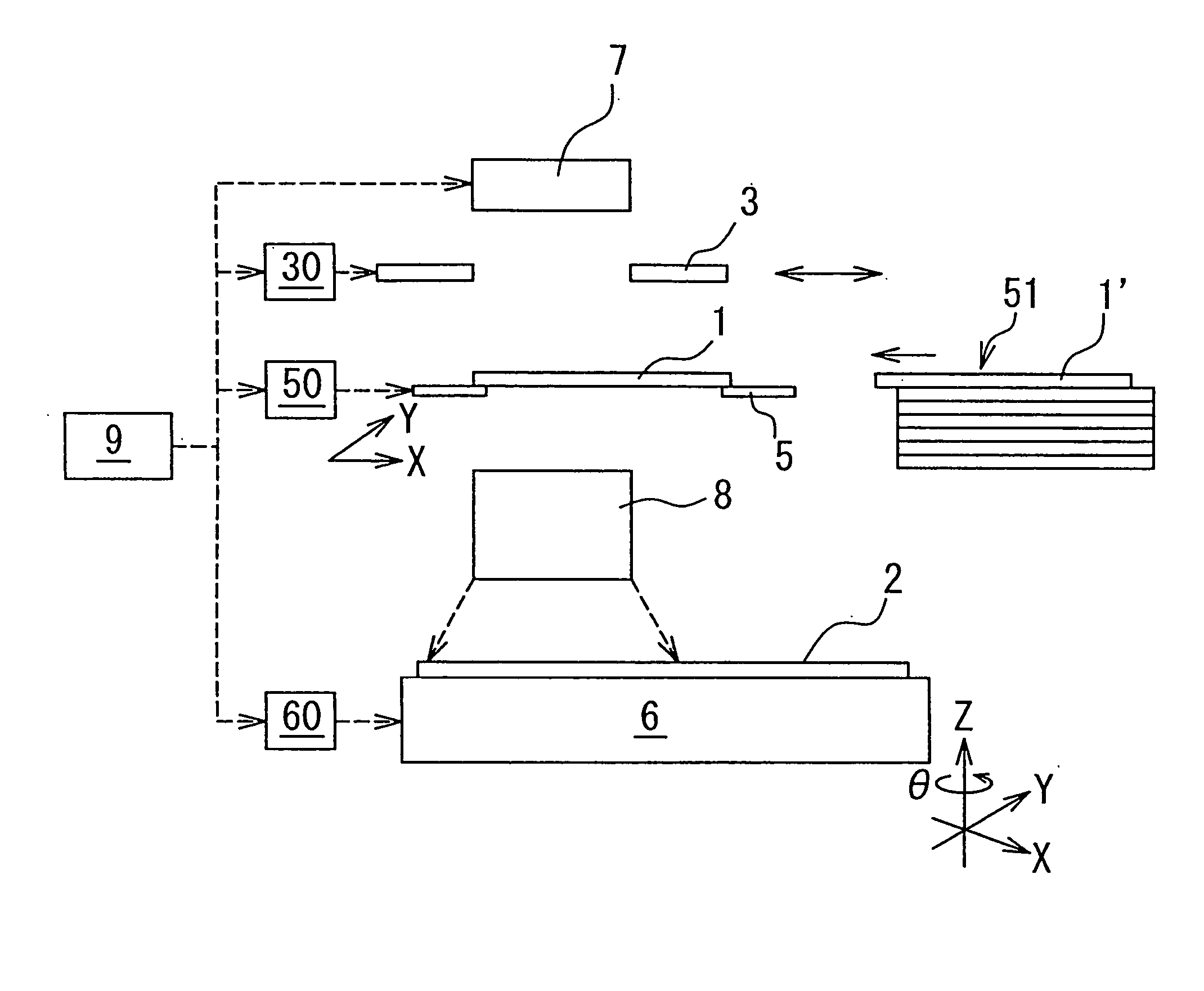
[0022] An embodiment of the invention will now be described in reference to the attached drawings. FIG. 1 shows a projection exposure device for producing a printed circuit board. A print circuit board 2 provided with photo resist is placed on a board stage 6 that is movable in the XYZ and θ directions by a board moving device 60.

[0023] A photo mask 1 on which circuit patterns are depicted is mounted on a photo mask stage 5 and faces to the print circuit board 2 in order to expose circuit patterns on the print circuit board 2 by an exposing light such as ultraviolet rays from a light source 7. The photo mask stage 5 is movable in XY direction by a photo mask moving device 50. The photo mask stage 5 is adapted to float by air pressure and be moved in a step by the photo mask moving device 50. The photo mask 1 is supplied and removed for changing to and from the photo mask stage 5 by a photo mask changer 51 that has a plurality of the photo mask 1′ in stock.

[0024] A masking device 3...


PUM


Abstract

A projection exposure apparatus and a method for producing a printed circuit board wherein, the whole pattern including pieces 10 and coupons 12 to be exposed on a print circuit board 2 is depicted on a photo mask 1 divided in six areas by divide line 19, the exposure will be made with respect to the each divided area of the photo mask 1 mounted on a movable photo mask stage 5 with using a masking device 3 masking other area than the exposing area.

Description

BACKGROUND OF THE INVENTION Field of the Invention and Related Art Statement [0001] The present invention relates to a projection exposure apparatus and a method for producing a printed circuit board. [0002] The photolithography method is applied widely in various fields, wherein a pattern is photographically imprinted by an exposure device on the surface of a board coated with photosensitive materials such as the photo resist, thereafter the pattern is formed on the board by etching process. Printed circuit boards are also fabricated by using the exposure device in recent years as shown in Japan Patent Laid-open No. 2000-250227 and Japan Patent Laid-open No. 2000-292942. [0003] Printed circuit boards become smaller as machines become miniaturized in recent years and for more efficient manufacturing process, a large-sized board is used. Such large-sized board is exposed with a plurality of the circuit and will be cut into small-sized boards in the following process. [0004] With such...

Claims


Application Information

Patent Timeline
IPC IPC(8): G03B27/42G03F7/20H05K3/00
CPCG03F1/14G03F7/2022H05K3/0002H05K2203/056H05K2201/09781H05K2201/09972H05K3/0082G03F7/20
Inventor NAKAGAWA, WATARUHASHIMOTO, KAZUNORI
Owner ADTEC ENG
Why Eureka
Try Eureka