Display device and driving method of the same

a technology of a display and a driving method, applied in the field of display devices, can solve the problems of reducing the contrast of a display, and achieve the effects of reducing the grayish black effect, reducing power consumption, and increasing contras

Active Publication Date: 2006-03-16
SEMICON ENERGY LAB CO LTD
View PDF40 Cites 16 Cited by
  • Summary
  • Abstract
  • Description
  • Claims
  • Application Information

AI Technical Summary

Benefits of technology

[0034] By using the first and second configurations in combination, an off current of the thin film transistor connected in series to the light emitting element continues to flow to the capacitor until it is charged. Therefore, longer time can be taken after selecting to turn off the thin film transistor connected in series to the light emit...

Problems solved by technology

Accordingly, there is a problem in...

Method used


Image

  • Display device and driving method of the same
  • Display device and driving method of the same
  • Display device and driving method of the same

Examples


embodiment mode 1

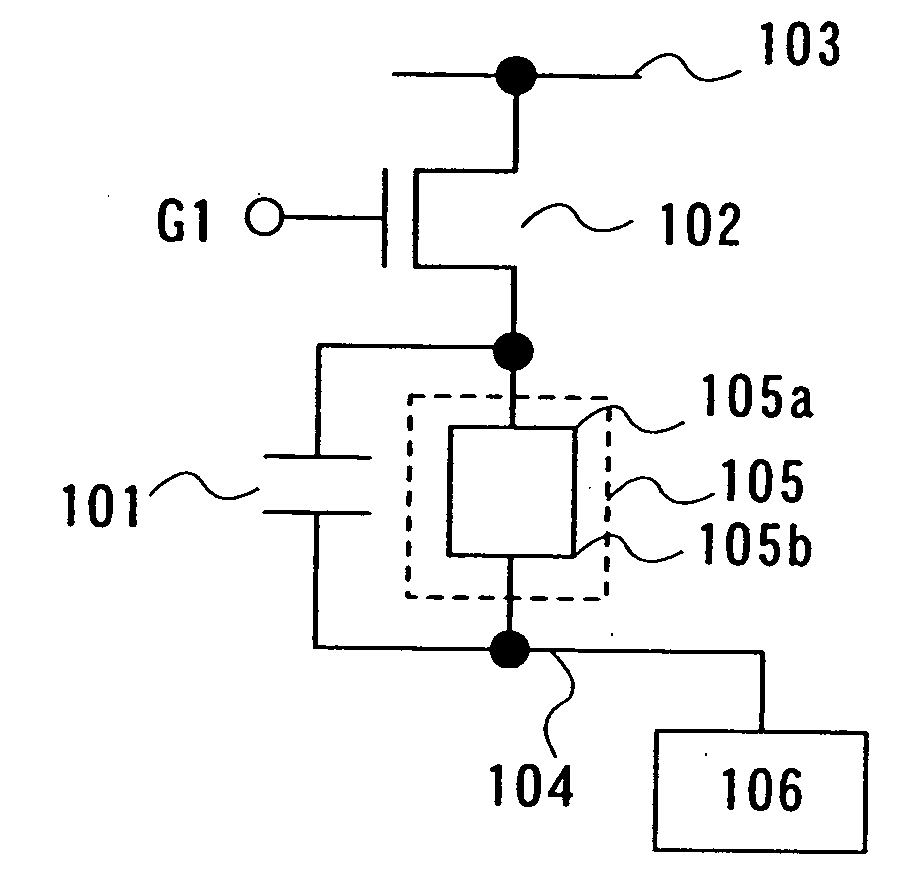
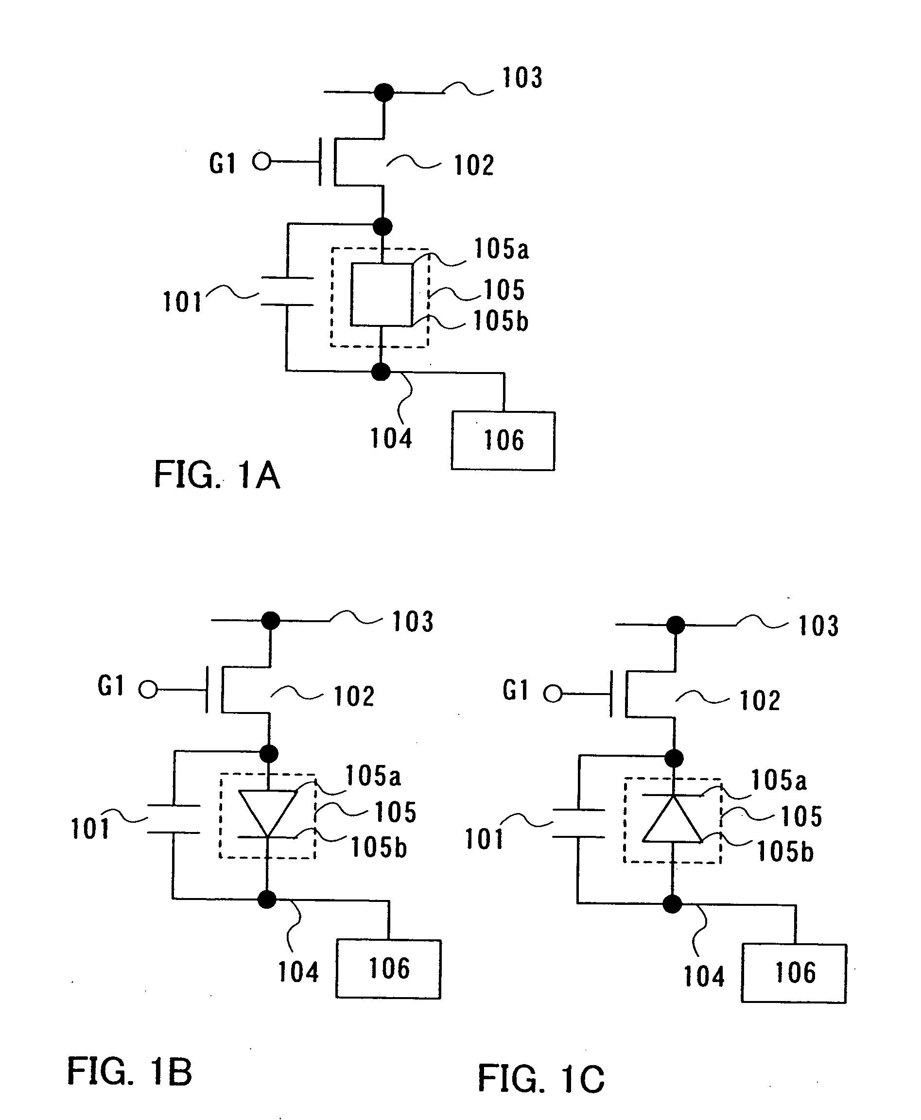
[0052] An example in which the first and third configurations are used in combination is described with reference to FIGS. 1A to 1C. In FIGS. 1A to 1C, reference numeral 105 denotes a light emitting element, 102 denotes a thin film transistor, 103 denotes a first power source line, 104 denotes a second power source line, 101 denotes a capacitor, and 106 denotes a circuit for setting a potential. The circuit 106 for setting a potential corresponds to the first configuration. The capacitor 101 corresponds to the third configuration. The light emitting element 105 has two electrodes and emits light at a luminance according to a current value of a current flowing between the two electrodes. One of the two electrodes of the light emitting element 105 is referred to as a first electrode 105a while the other is referred to as a second electrode 105b.

[0053] A method for using the first and third configurations in combination is described with reference to FIG. 1A.

[0054] When the thin film...

embodiment mode 2

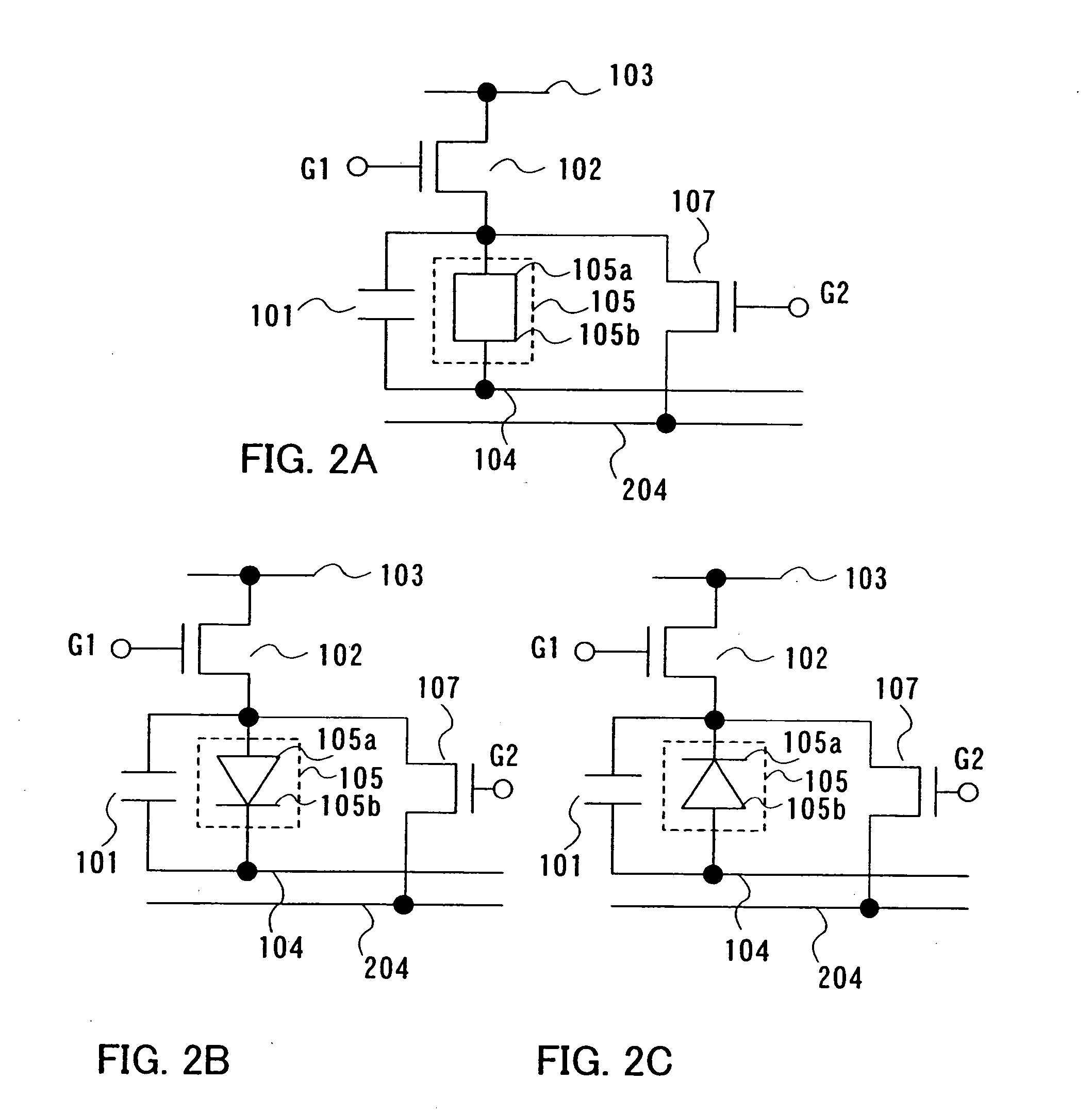
[0066] An example of using the second and third configurations in combination is described with reference to FIGS. 2A to 2C. In FIGS. 2A to 2C, the same reference numerals are used for the same portions as in FIGS. 1A to 1C, and a description thereon is omitted. Reference numeral 107 denotes a thin film transistor. The thin film transistor 107 and a third power source line 204 correspond to the second configuration. The capacitor 101 corresponds to the third configuration.

[0067] A method for using the second and third configurations in combination is described in details with reference to FIG. 2A.

[0068] When the thin film transistor 102 connected in series to the light emitting element 105 is selected to be turned off, the thin film transistor 107 is selected to be turned on by controlling a potential G2 applied to a gate thereof. In this manner, a potential of the third power source line 204 is applied to the first electrode 105a. When the thin film transistor 107 is selected to ...

embodiment mode 3

[0074] An example of using the first and third configurations in combination is described with reference to FIGS. 3A to 3D. In FIGS. 3A to 3D, the same reference numerals are used for the same portions as in FIGS. 1A to 1C and a description thereon is omitted.

[0075] Each of FIGS. 3A and 3B corresponds to FIG. 1A provided with the capacitor 108. The capacitor 108 is provided to hold a gate-source voltage of the thin film transistor 102. FIG. 3A shows an example where the thin film transistor 102 has a source on a side connected to the first power source line 103. FIG. 3B shows an example where the thin film transistor 102 has a source on a side connected to the first electrode 105a of the light emitting element 105.

[0076] A drain current of the thin film transistor 102 changes according to a potential difference between a source potential thereof and the gate potential G1. Even if the gate potential G0 of the thin film transistor 102 is controlled, when a source potential changes, ...


PUM


Abstract

A problem in that a light emitting element slightly emits light is solved by an off current of a thin film transistor connected in series to the light emitting element, thereby a display device which can perform a clear display by increasing contrast, and a driving method thereof are provided. When the thin film transistor connected in series to the light emitting element is turned off, a charge held in the capacitance of the light emitting element itself is discharged. Even when an off current is generated at the thin film transistor connected in series to the light emitting element, this off current charges this capacitance until the capacitance of the light emitting element itself holds a predetermined voltage again. Accordingly, the off current of the thin film transistor does not contribute to light emission. In this manner, a slight light emission of the light emitting element can be reduced.

Description

BACKGROUND OF THE INVENTION [0001] 1. Field of the Invention [0002] The present invention relates to a display device of an active matrix driving method in which a switching element is provided in each pixel, and a driving method thereof. In particular, the invention relates to a display device in which a luminance of a light emitting element is controlled by controlling a current supplied to the light emitting element by using a switching element connected in series to the light emitting element, and a driving method thereof. More particularly, the invention relates to a display device including an element with diode characteristics as a light emitting element and a driving method thereof. [0003] 2. Description of the Related Art [0004] A display device including a thin film transistor as a switching element and a driving method thereof are suggested. FIG. 8A shows an example of a pixel configuration thereof. [0005] In FIG. 8A, reference numeral 105 denotes a light emitting element...

Claims


Application Information

Patent Timeline
IPC IPC(8): H01L29/04H05B44/00
CPCG09G3/3233G09G3/3241G09G2300/0842G09G2300/0852G09G2310/0256H01L27/156G09G2320/0238H01L27/3244H01L27/3248H01L27/3265G09G2320/02H10K59/123H10K59/1216G09G3/30H05B33/00H10K59/12
Inventor MIYAKE, HIROYUKIIWABUCHI, TOMOYUKIFUKUMOTO, RYOTA
Owner SEMICON ENERGY LAB CO LTD
Why Eureka
Try Eureka