Chip package assembly produced thereby

a technology of chip package and assembly, applied in the direction of semiconductor devices, electrical devices, semiconductor/solid-state device details, etc., can solve the problems of poor image sensitivity of the camera module, csp device, and failure to provide good light convergence capacity, etc., to save cost, increase yield rate, and high image sensitivity

Inactive Publication Date: 2006-03-16
AU OPTRONICS CORP
View PDF41 Cites 12 Cited by
  • Summary
  • Abstract
  • Description
  • Claims
  • Application Information

AI Technical Summary

Benefits of technology

[0008] The primary object of the invention is therefore to specify a chip package assembly, in order to save the cost, to increase the yield rate and to provide high image sensitivity.

Problems solved by technology

How to increase the production mass of and how to keep the quality of the component packages are the current issues.
However, the optical paste 50a is filled between the chip 20a and the cover glass 40a, according to Snell's Law, the light passes through the cover glass 40 and is transmitted into the μ-lens array 21a via the optical paste 50a, and the CSP device 1a fails to provide good light convergence capacity and the image sensitivity of the camera module is bad.
In addition, the CSP device 1a is obviously difficult to manufacture due to the complicated structure per se and the complex steps, the yield rate cannot raise so that the materials and the cost cannot be saved.
During the COB processes, if there is any particle or dust fallen on the μ-lens array 21b of the chip 20b, a kind of critical failure mode will damage the image sensing, the fallen particle cannot be removed by any cleaning means, and therefore, the camera module absolutely fails.
But such the clean room is so expensive, and the lager size of the clean room for containing all the equipments used in the COB processes costs more than the regular one.
Nevertheless, the wire bonding procedure causes the air disturbance due to the high speed thereof.

Method used


Image

  • Chip package assembly produced thereby
  • Chip package assembly produced thereby
  • Chip package assembly produced thereby

Examples


Embodiment Construction

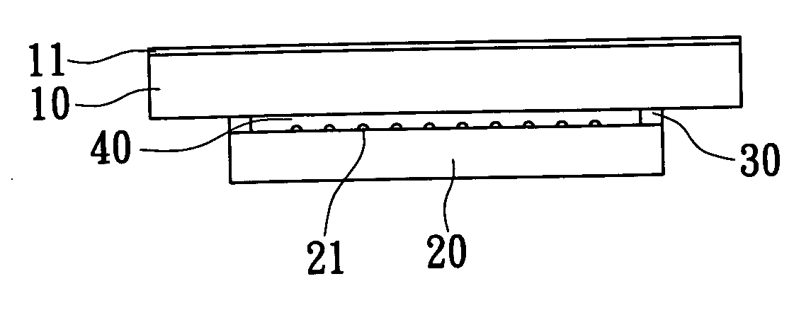
[0025] With respect to FIGS. 3A to 3F, a chip package assembly is disclosed. The chip package assembly (in FIG. 3A) includes a transparent substrate 10 having a first surface and a circuit layout 12 planted on a predetermined region of the first surface for electrical connection, a chip 20 arranged beneath the transparent substrate 10, and a joint pad 30 connecting the circuit layout 12 of the transparent substrate 10 and the chip 20. The joint pad 30 illustrated in FIG. 3B according to an embodiment is arranged in a discontinuous manner, and the chip package assembly further includes a sealing paste 50 coated around the joint pad 30 for connecting the joint pad 30, the chip 20 and the transparent substrate 10 simultaneously, so as to form an unoccupied layer 40 sealed up and isolated between the chip 20 and the transparent substrate 10 for high image sensitivity. The joint pad 30 illustrated in FIG. 3D according to another embodiment is circled and arranged in a continuous manner, ...


PUM


Abstract

A chip package assembly is rather than a conventional package assembly and can improve the ability of packaging a photoelectric chip in order to save materials and costs. The chip package assembly includes a transparent substrate, a chip is electrically connected to a circuit layout of the transparent substrate, a joint pad arranged therebetween. Make sure an unoccupied layer is sealed up between the transparent substrate and the chip, so as to form the chip package assembly. After the processes mentioned above are done, the chip package assembly can leave the clean room to run post-processes, such as die sawing, or camera module packaging.

Description

BACKGROUND OF THE INVENTION [0001] 1. Field of the Invention [0002] The present invention relates to a chip package assembly, and particularly relates to a chip package assembly that is rather than conventional package assemblies and can improve the ability of packaging an optical electronic sensor, for example, the optical electronic sensor connects a predetermined region of a circuit layout of a transparent sheet via a conductive material, in order to form an unoccupied layer therebetween. After each chip is packaged, the transparent sheet is sawed into plurality of dices, the dices can be assembled into various camera module. [0003] 2. Description of Related Art [0004] As much progress of electronic products does, such as being lightweight, thin, short and small, and being multiple functions, component packages applied for these electronic products develop with high frequency, quantities of I / O ports and microminiaturize. How to increase the production mass of and how to keep the...

Claims


Application Information

Patent Timeline
Patent Type & Authority Applications(United States)
IPC IPC(8): H01L23/02H01L31/0203H01L31/0232H04N1/028
CPCH01L27/14618H01L31/0203H01L2224/16H01L2224/48091H01L2224/48227H01L2924/00014H01L2224/16225H01L2224/32225H01L2224/73204H01L2924/00011H01L2224/0401H01L2924/00
Inventor TIAO, KUO-TUNG
Owner AU OPTRONICS CORP
Why Eureka
Try Eureka