Stacked board-on-chip package having mirroring structure and dual inline memory module on which the stacked board-on-chip package are mounted

Inactive Publication Date: 2006-03-16
SAMSUNG ELECTRONICS CO LTD
View PDF6 Cites 31 Cited by
  • Summary
  • Abstract
  • Description
  • Claims
  • Application Information

AI Technical Summary

Problems solved by technology

When DIMMs are constructed with a conventional stacked BOC package 100, signal fidelity cannot be ensured because of the increased load of the signal line.
Hence, it is not easy to apply an optimal topology to the DIMM.
Developing an extra package increases costs.

Method used


Image

  • Stacked board-on-chip package having mirroring structure and dual inline memory module on which the stacked board-on-chip package are mounted
  • Stacked board-on-chip package having mirroring structure and dual inline memory module on which the stacked board-on-chip package are mounted
  • Stacked board-on-chip package having mirroring structure and dual inline memory module on which the stacked board-on-chip package are mounted

Examples


Embodiment Construction

[0023] The attached drawings illustrating preferred embodiments of the present invention are referred to in order to gain a better understanding of the present invention, the merits thereof, and the objectives accomplished thereby.

[0024] Hereinafter, the present invention will be described in detail by explaining preferred embodiments of the invention with reference to the attached drawings. Like reference numerals in the drawings denote like elements.

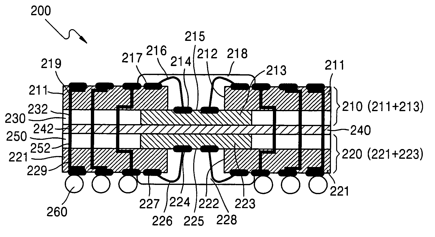
[0025]FIG. 2 illustrates a stacked board-on-chip (BOC) package 200 having a mirroring structure, according to an exemplary embodiment of the present invention. Referring to FIG. 2, the stacked BOC package 200 is obtained by sequentially stacking a first package 210, a first interposer 230, a heat spread plate 240, a second interposer 250, and a second package 220. As will be described, each of the first and second interposers 230 and 250 has a structure that permits the first and second packages 210 and 220 to be electrically connect...


PUM


Abstract

Embodiments of the invention include a stacked board-on-chip (BOC) package having a mirroring structure and a dual inline memory module (DIMM) on which the stacked BOC package is mounted. A bottom surface of a first semiconductor chip faces a bottom surface of a second semiconductor chip. An interposer electrically connects first and second packages, respectively comprising the first and second semiconductor chips, to each other. The DIMM is obtained by electrically connecting BOC packages to each other on upper and lower substrates of a printed circuit board. Since a height of the stacked BOC packages is greater than a height of a conventional stacked BOC package, the DIMM has a minimum stub length and an optimal topology. Hence, the DIMM can have a signal with excellent fidelity by reducing a load upon a signal line, and installation or wiring of components within the DIMM 300 requires less effort.

Description

BACKGROUND OF THE INVENTION [0001] This application claims the benefit of Korean Patent Application No. 10-2004-0072471, filed on Sep. 10, 2004, in the Korean Intellectual Property Office, the disclosure of which is incorporated herein in its entirety by reference. [0002] 1. Field of the Invention [0003] The present invention relates to a semiconductor package, and more particularly, to a stacked board-on-chip (BOC) package having a mirroring structure and a dual inline memory module (DIMM) on which the stacked BOC packages are mounted. [0004] 2. Description of the Related Art [0005] The trend in the semiconductor industry is to make semiconductor products compact, thin, light, highly integrated, and highly densified. This trend is also applied to dual inline memory modules (hereinafter, referred to as DIMMs) on each of which semiconductor memory devices are mounted. Board-on-chip (BOC) packages are well known and used for, for example, high-speed dynamic random access memory (DRAM)...

Claims


Application Information

Patent Timeline
IPC IPC(8): H01L23/02
CPCH01L23/3128H01L25/105H01L2224/4824H01L2924/15311H01L2924/15331H01L2924/19041H01L2224/06136H01L2225/1094H01L2224/48091H01L2225/1023H01L2225/107H01L25/16H01L2924/00014H01L23/12H01L25/00
Inventor CHO, JEONG-HYEONLEE, JUNG-JOONKIM, DO-HYUNGSO, BYUNG-SE
Owner SAMSUNG ELECTRONICS CO LTD
Why Eureka
Try Eureka