Thin glass chip for an electronic component and manufacturing method

a technology of electronic components and manufacturing methods, applied in glass shaping apparatus, decorative surface effects, decorative arts, etc., can solve the problems of large loss of mechanical strength of wafers, risk of cracks or breaks of components formed at the front surface, and small thickness desired for final components, etc., to achieve the effect of suppressing the risk

Active Publication Date: 2006-03-16
STMICROELECTRONICS SRL
View PDF5 Cites 152 Cited by
  • Summary
  • Abstract
  • Description
  • Claims
  • Application Information

AI Technical Summary

Benefits of technology

[0011] An aspect of the present invention aims at suppressing the risk entailed by the handling of thin wafers, especially made of glass, at the end of a manufacturing process of electronic components and more specifically of components formed on a single surface with thick or stressful processings likely to generate surface evenness defects of the wafer.

Problems solved by technology

The small thickness desired for the final components is, however, incompatible with the stress undergone by the wafers during manufacturing, and the final thickness of the individual substrate of the component is accordingly achieved at the end of the process.
At the end of the thickness reduction, the wafer considerably loses its mechanical strength.
Now, the handlings required in subsequent steps, among others of cleaning and washing, resulting in risks of cracks or breaks of the structures of the component formed at the front surface.
It should be noted that this risk of breakage of the structure is already present in the rectification step, due to the irregular bearing of the front surface which supports the components.
The irregular bearing resulting therefrom, associated with the pressure applied by the grinding wheel on the rear surface, causes breakage risks, especially at the end of the rectification step when the wafer becomes thinner and thinner and this thickness difference is no longer negligible as compared with the general wafer thickness.
Another disadvantage is linked to a deformation of the wafer which becomes slightly bulged (warp) when it is thin.
This curvature may impede the wafers from being housed in batch processing baskets.
As an example, with a deflection reaching 3.2 mm, the introduction of the thin wafers in usual handling baskets is no longer possible.

Method used


Image

  • Thin glass chip for an electronic component and manufacturing method
  • Thin glass chip for an electronic component and manufacturing method
  • Thin glass chip for an electronic component and manufacturing method

Examples


first embodiment

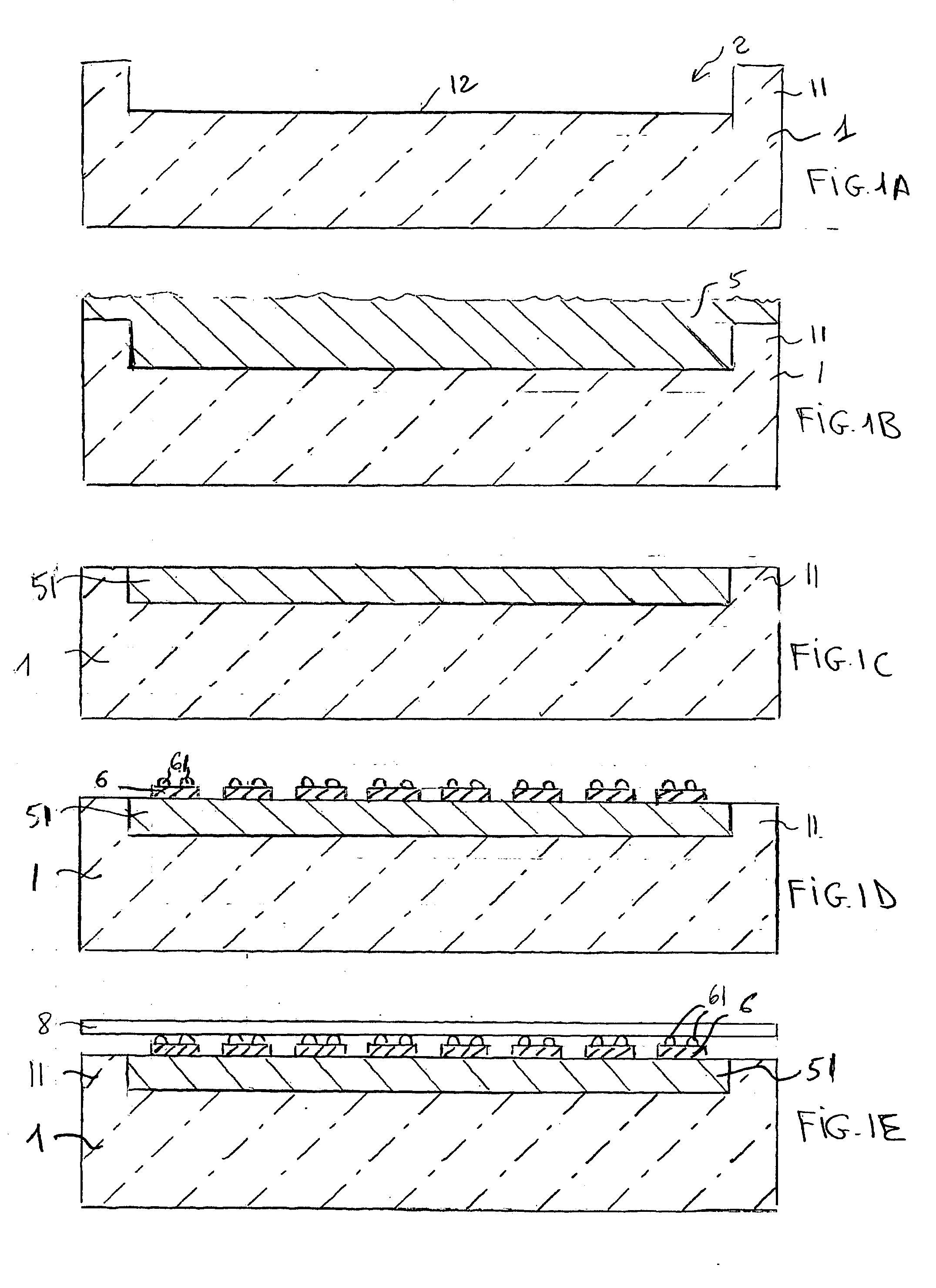
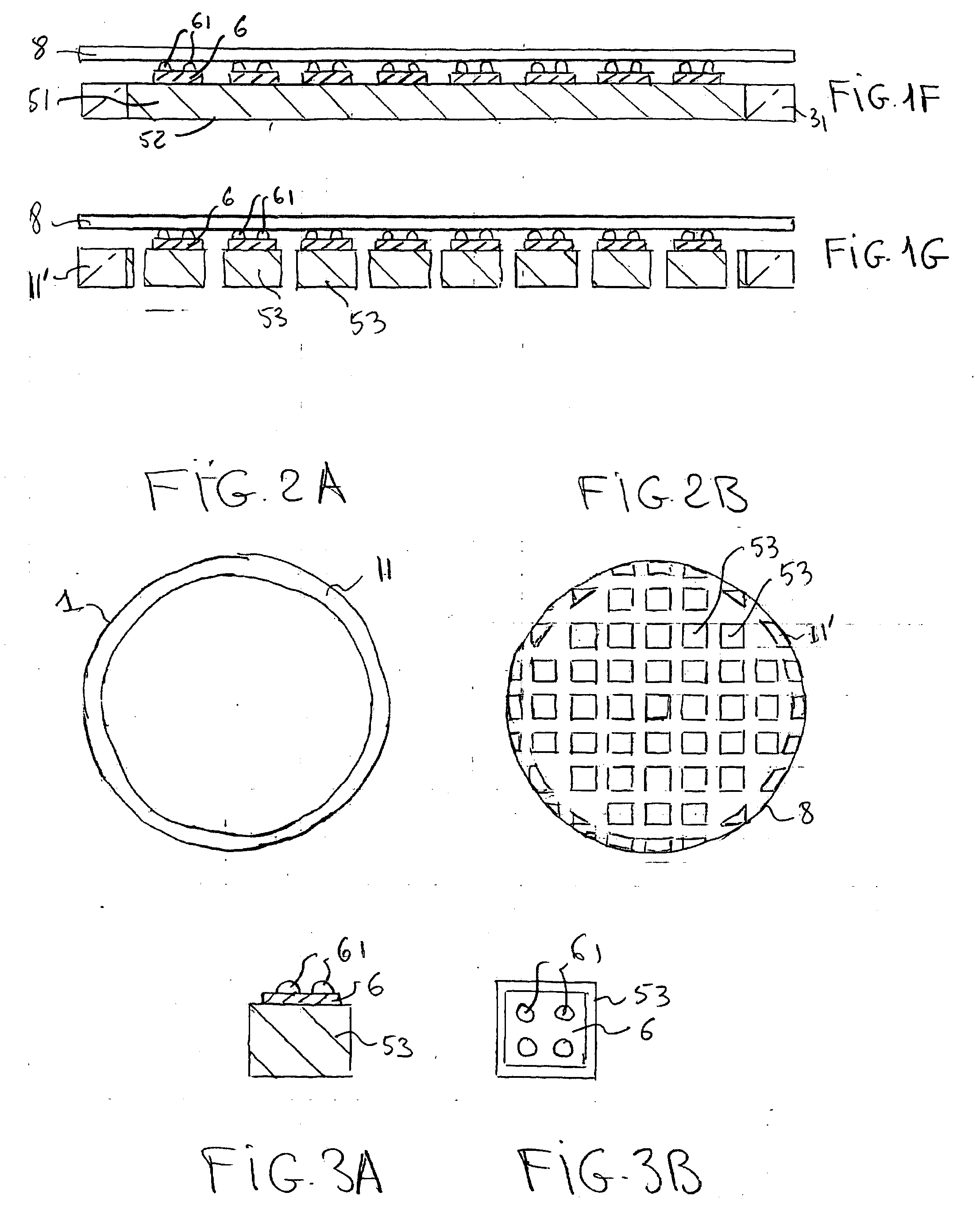
[0038]FIGS. 1A TO 1G illustrate, in simplified cross-sectional views, a method for manufacturing passive components on insulating substrates, preferably made of glass, according to the present invention.

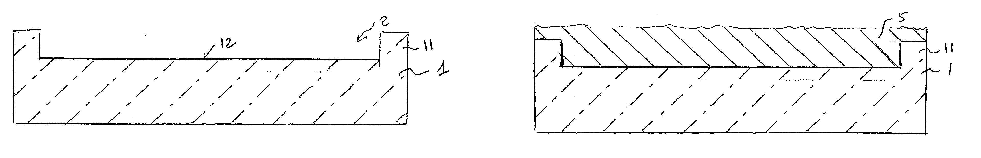
[0039] It is started from a silicon wafer 1 (or another material currently used as a substrate in the electronic industry, preferably, of low cost). An etch, preferably circular, is performed in wafer 1, to obtain a peripheral silicon wall 11 surrounding the disk-shaped bottom 12 of the performed etch. FIG. 2A shows a top view of this structure.

[0040] According to an embodiment of the present invention, the depth of the obtained cavity 2 is selected to correspond (at least approximately) to the final thickness desired for the glass substrates intended to support the components formed at the front surface. For example, the etch depth ranges between 20 and 100 μm while the total thickness of wafer 1 is initially greater than the etched depth (for example, 500 μm).

[0041] The function ...


PUM

PropertyMeasurementUnit
thicknessaaaaaaaaaa
depthaaaaaaaaaa
thicknessaaaaaaaaaa

Abstract

The manufacturing of electronic components on individual substrates made of an insulating material includes molding, in a silicon wafer, an insulating material with a thickness corresponding to the final thickness desired for the substrates, manufacturing the electronic components, and removing the silicon from the rear surface of the wafer after manufacturing of the components.

Description

PRIORITY CLAIM [0001] This application claims priority from French patent application No. 04 / 52039, filed Sep. 14, 2004, which is incorporated herein by reference. BACKGROUND OF THE INVENTION [0002] 1. Field of the Invention [0003] The present invention relates to the manufacturing of electronic components on wafers used as a substrate and, more specifically, to so-called single face products, that is, having their components supported by a single surface of the wafer. [0004] The present invention more specifically applies to the manufacturing of passive components on glass substrates. [0005] 2. Discussion of the Related Art [0006] The search for component miniaturization goes along with a need to reduce the thickness of the wafers or substrates supporting these components. The small thickness desired for the final components is, however, incompatible with the stress undergone by the wafers during manufacturing, and the final thickness of the individual substrate of the component is...

Claims


Application Information

Patent Timeline
Patent Type & Authority Applications(United States)
IPC IPC(8): H01L21/50H01L21/48H01L21/44B29C33/42C03B11/08H01L27/13
CPCH01L21/6835H01L2924/01033H01L21/78H01L24/97H01L2221/68327H01L2221/68354H01L2221/68363H01L2221/68377H01L2224/16H01L2924/01079H01L2924/19041H01L2924/19042H01L2924/19043H01L2924/30107H01L2924/01006H01L21/6836H01L2924/00014H01L2924/00011H01L2224/0401
Inventor GARDES, PASCALGUITTON, FABRICE
Owner STMICROELECTRONICS SRL
Why Eureka
Try Eureka