
Process and fabrication methods for emitter wrap through back contact solar cells

a solar cell and emitter wrap technology, applied in the field of methods and processes for fabricating backcontact silicon solar cells, solar cells, etc., can solve the problems of low-cost process sequence, significantly poor conductivity of alloyed-al grid cells, etc., and achieve low cost and high efficiency. , the effect of fewer process steps

Inactive Publication Date: 2006-03-23
APPLIED MATERIALS INC
View PDF99 Cites 232 Cited by
  • Summary
  • Abstract
  • Description
  • Claims
  • Application Information

AI Technical Summary

Benefits of technology

[0028] An advantage of the present invention is that it provides for manufacturing processes with fewer, more economical process steps that produce high efficiency solar cells.

Problems solved by technology

The resulting cell suffered from significantly poor conductivity of the alloyed-Al grid.
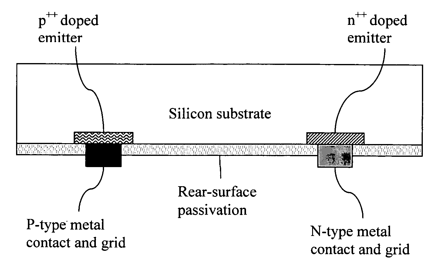
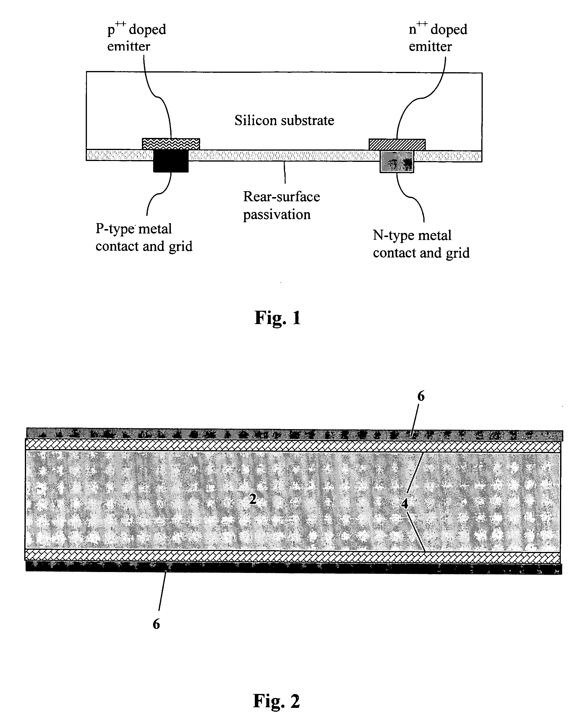
A critical issue for any back-contact silicon solar cell is developing a low-cost process sequence that also electrically isolates the negative and positive polarity grids and junctions.
The technical issue includes patterning of the doped layers (if present), passivation of the surface between the negative and positive contact regions, and application of the negative and positive polarity contacts.

Method used


Image

  • Process and fabrication methods for emitter wrap through back contact solar cells
  • Process and fabrication methods for emitter wrap through back contact solar cells
  • Process and fabrication methods for emitter wrap through back contact solar cells

Examples


first embodiment

[0139] In a first embodiment, the grid lines are made with a tapered width—such that the width is increased along the direction of current flow until it reaches the edge of the cell. This reduces the series resistance at a constant grid coverage fraction because the cross-sectional area of the grid increases at the same rate that the current carried by the grid increases. A preferred embodiment of the tapered width pattern in both positive-polarity current-collection grid 510 and negative-polarity current-collection grid 520 is shown in FIG. 22 (not to scale). FIG. 23 shows a cross-sectional view of the IBC grids of FIG. 22 on the back surface of solar cell 505 with plated metallization; that is, metal 530 plated over the contact metallizations.

[0140] In general, the degree of tapering may be determined either empirically or by calculation, to determine an optimal tapering. Additionally, the metal coverage fraction and the spacing between same-polarity grids may similarly be varied....

second embodiment

[0141] In a second embodiment, the grid resistance can be reduced by making the grid lines thicker. The thickness of screen-printed Ag paste grids is limited by the physical properties of the paste and screen. The preferred geometry for the IBC grid permitting edge collection (FIG. 19A) typically requires relatively thick grid lines (>50 μm) in order to be able to conduct current over the large dimensions with acceptable resistance losses. This is thicker than can be easily screen printed. Two preferred methods of increasing the grid line thickness of the printed Ag IBC grid are: by dipping the IBC cell into molten solder (“tin dipping”) or by plating (electro- or electroless) of metal onto the grid lines. Tin dipping is a well known process that is used by some silicon solar cell manufacturers for fabrication of conventional silicon solar cells. The temperature of the molten solder depends upon the composition of the solder, but is generally less than 250° C. In one embodiment a Sn...


PUM


Abstract

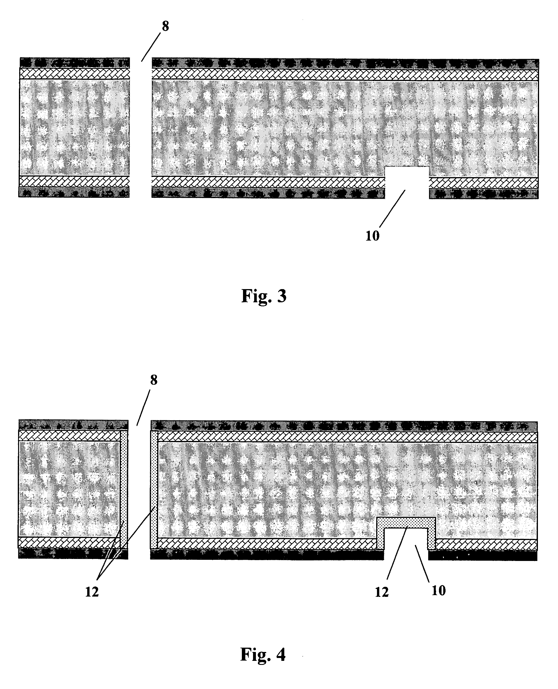
Back contact solar cells including rear surface structures and methods for making same. The rear surface is doped to form an n+ emitter and then coated with a dielectric layer. Small regions are scribed in the rear surface and p-type contacts are then formed in the regions. Large conductive grid areas overlay the dielectric layer. The methods provide for increasing efficiency by minimizing p-type contact areas and maximizing n-type doped regions on the rear surface of a p-type substrate.

Description

CROSS-REFERENCE TO RELATED APPLICATIONS [0001] This application claims priority to and the benefit of the filing of U.S. Provisional Patent Application Ser. No. 60 / 607,984, entitled “Improved Process and Fabrication Methods for Emitter Wrap Through Back Contact Solar Cells,” filed on Sep. 7, 2004, and U.S. Provisional Patent Application Ser. No. 60 / 707,648, entitled “Further Improved Process and Fabrication Methods for Emitter Wrap Through Back Contact Solar Cells,” filed on Aug. 11, 2005. This application is also a continuation-in-part application of the following U.S. Patent Applications, all of which were filed on Feb. 3, 2005: Ser. No. 11 / 050,185, entitled “Back-Contact Solar Cells and Methods for Fabrication”; Ser. No. 11 / 050,182, entitled “Buried-Contact Solar Cells With Self-Doping Contacts”; and Ser. No. 11 / 050,184, entitled “Contact Fabrication of Emitter Wrap-Through Back Contact Silicon Solar Cells”, which applications claim the benefit of the filing of U.S. Provisional P...

Claims


Application Information

Patent Timeline
IPC IPC(8): H01L31/00
CPCH01L31/068Y02E10/547H01L31/022458H01L31/1804H01L31/0682Y02P70/50H01L31/04
Inventor HACKE, PETERGEE, JAMES M.
Owner APPLIED MATERIALS INC
Learn More