

Microstructures and method of manufacture
a microstructure and manufacturing method technology, applied in the field of microstructures, can solve the problems of poor signal strength reproducibility, small signal strength, and insufficient resonance intensity, and achieve excellent reproducibility and increase sensitivity
Inactive Publication Date: 2006-03-23
FUJIFILM HLDG CORP +1
View PDF3 Cites 37 Cited by
- Summary
- Abstract
- Description
- Claims
- Application Information
AI Technical Summary
Benefits of technology
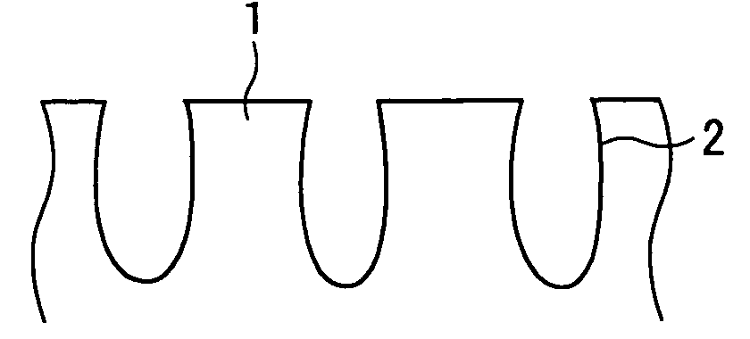
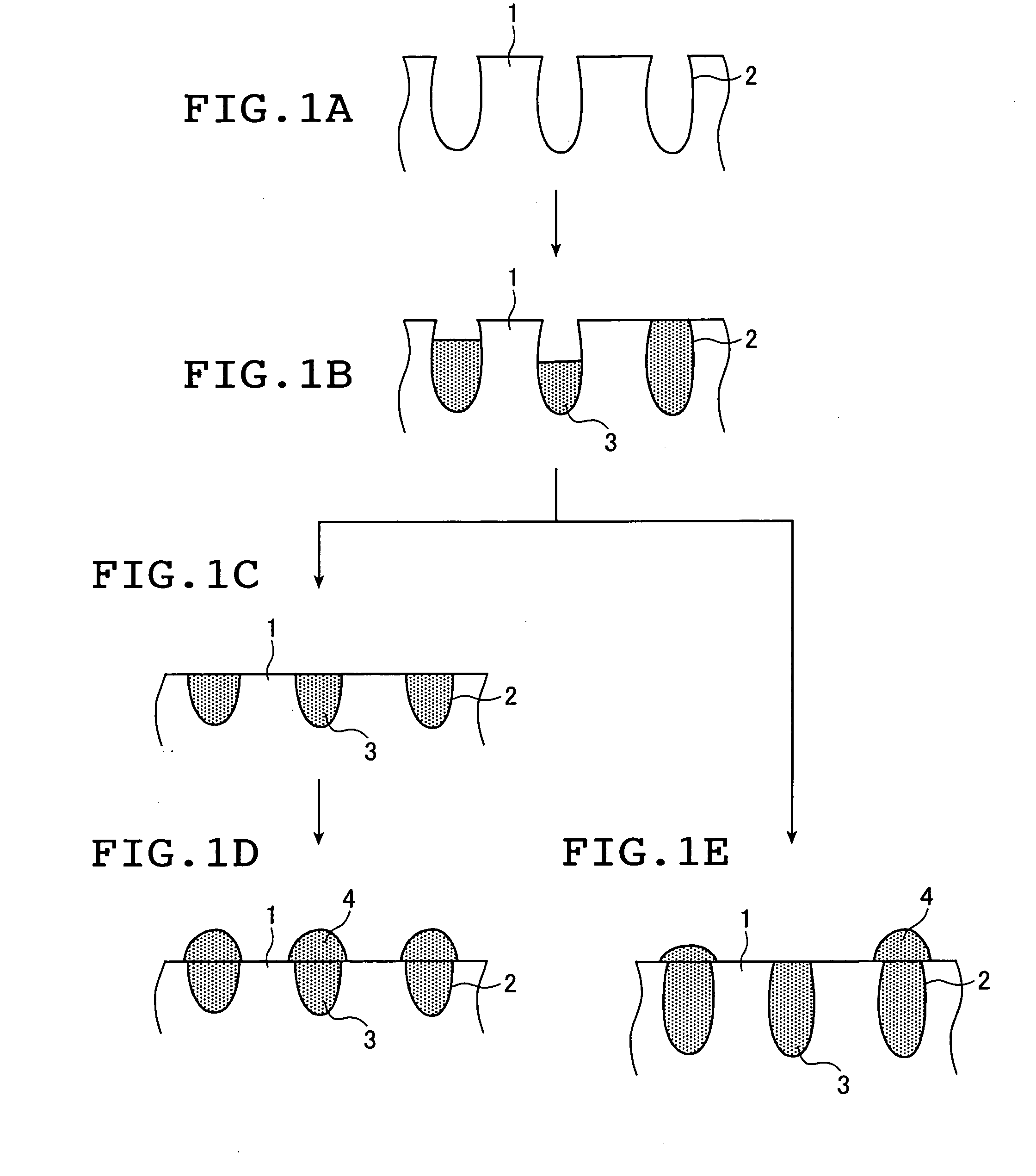
[0020] It is therefore an object of the present invention to provide a structure which has a sufficiently large signal strength and generates local plasmon resonance of excellent reproducibility.
[0022] We have discovered as well that, in devices which use a self-ordered anodized layer, by removing at least a portion of the anodized layer and conferring the layer with a predetermined average surface roughness (Ra), the irregularities in the filling of micropores with metal that occur during sealing treatment can be eliminated. As a result, the signal strength can be made sufficiently large, enabling an excellent reproducibility to be achieved.
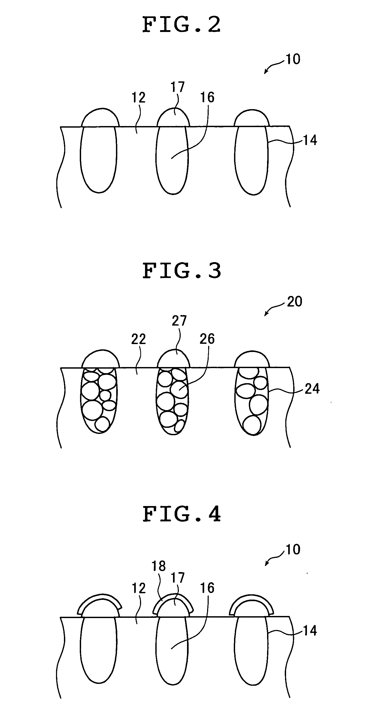
[0033] When the structure of the invention is used as a sample holder for Raman spectroscopy, because the metal particles are in close proximity and uniformly present on the structure, the local plasmon resonance is larger, greatly increasing the sensitivity and providing an excellent reproducibility.
Problems solved by technology
As a result, we have discovered that in prior-art devices which employ a self-ordered anodized layer, the resonance intensity is not sufficiently large.
However, we have found that when the resulting plasmon resonance device is used as a sample holder for Raman spectroscopy, signal strength reproducibility is poor.
We have also found from additional studies that when a plasmon resonance device is used as a sample holder for Raman spectroscopic analysis, if a liquid sample to be analyzed does not adhere to the surface of the metal particles or adheres but does so non-uniformly, the signal strength becomes small or the signal reproducibility worsens.
Method used
View moreImage
Smart ImageViewing Examples

Examples
examples
[0186] Examples are given below by way of illustration and should not be construed as limiting the invention.
Login to View More PUM
| Property | Measurement | Unit |
|---|---|---|
| Fraction | aaaaa | aaaaa |
| Fraction | aaaaa | aaaaa |
| Diameter | aaaaa | aaaaa |
Abstract
In order to provide a structure which has a sufficiently large signal strength and generates local plasmon resonance of excellent reproducibility, the invention provides a process for manufacturing a structure at least a portion of which is an aluminum member having on a surface thereof an anodized layer having a plurality of micropores, the process comprising the steps of, in order, anodizing a surface of an aluminum member so as to form an anodized layer having micropores present therein, sealing the micropores in the anodized layer by filling the micropores with metal, surface-treating the sealed anodized layer so as to remove at least a portion of upper layer surface thereof and set the average surface roughness (Ra) to at most 30 nm, and subjecting the surface-treated anodized layer to electrodeposition so as to form metal particles on the metal filled into the micropores during sealing.
Description
[0001] The entire contents of literatures cited in this specification are incorporated herein by reference. BACKGROUND OF THE INVENTION [0002] The present invention relates to a microstructure which uses an aluminum member having on a surface thereof an anodized layer having a plurality of micropores. The invention also relates to a process for manufacturing such a microstructure. [0003] Within technical fields having to do with, for example, metal and semiconductor thin films, fine lines and dots, it is known that the movement of free electrons becomes confined at sizes smaller than some characteristic length, as a result of which peculiar electrical, optical and chemical phenomena become observable. Such phenomena are called “quantum-mechanical size effects” or simply “quantum size effects.” Active research and development is currently being conducted on functional materials which employ such phenomena. Specifically, materials having structures smaller than several hundred nanomet...
Claims
Login to View More Application Information
Patent Timeline
 IPC IPC(8): C25D11/20
CPCC25D11/18
InventorTOMITA, TADABUMIHOTTA, YOSHINORIUESUGI, AKIO
OwnerFUJIFILM HLDG CORP