Scanning electron microscope

a scanning electron microscope and electron microscope technology, applied in the direction of material analysis using wave/particle radiation, instruments, nuclear engineering, etc., can solve the problems of limited to a few routinely used add-ons, difficult detection and analysis, and little space in this design for mounting detectors and spectrometers, and achieve high transport efficiency

Active Publication Date: 2006-03-23
NAT UNIV OF SINGAPORE
View PDF3 Cites 120 Cited by
  • Summary
  • Abstract
  • Description
  • Claims
  • Application Information

AI Technical Summary

Benefits of technology

[0012] SEMs that do not restrict detectors or spectrometers to be located in the small space between a conventional SEM objective lens and the specimen are disclosed. These SEMs are predicted to have high transport efficiency for all scattered electrons and photons, from the specimen to their respective detectors.

Problems solved by technology

In principle, many analytical techniques can be combined with the normal operation of a SEM, but in practice, they are limited to a few routinely used add-on attachments.
Unfortunately, most of the electrons and photons that are scattered back from the sample travel back towards the column and are therefore difficult to detect and analyze.
There is therefore little room in this design to mount detectors and spectrometers that can efficiently collect the secondary electrons and photons generated by the primary beam-specimen interaction or analyze their energy spectra with high resolution.
This off-axis position, however, results in poor collection efficiency for the secondary electrons, typically well below 50% in most conventional SEMs.
In general, the mixing of secondary electrons and BSEs is undesirable since BSEs provide poorer spatial resolution than secondary electrons.
Although EDS, WDS or CL attachments are very useful, conventional SEM designs are not optimized for their use, precisely for the same reasons that preclude the high efficiency collection of secondary electrons and BSEs.
There are several instances where energy filtering of the scattered electrons provides important analytical information about the sample, however, the difficulty of employing high resolution spectrometers into conventional SEMs is well documented in L. Reimer, Scanning Electron Microscopy, Physics of Image Formation and Microanalysis, 2nd edition, chapter 5: Electron Detectors and Spectrometers, pp.
Although a variety of different electron / energy detectors have been proposed, no SEM capable of using a variety of detectors has emerged.

Method used


Image

  • Scanning electron microscope
  • Scanning electron microscope
  • Scanning electron microscope

Examples


Embodiment Construction

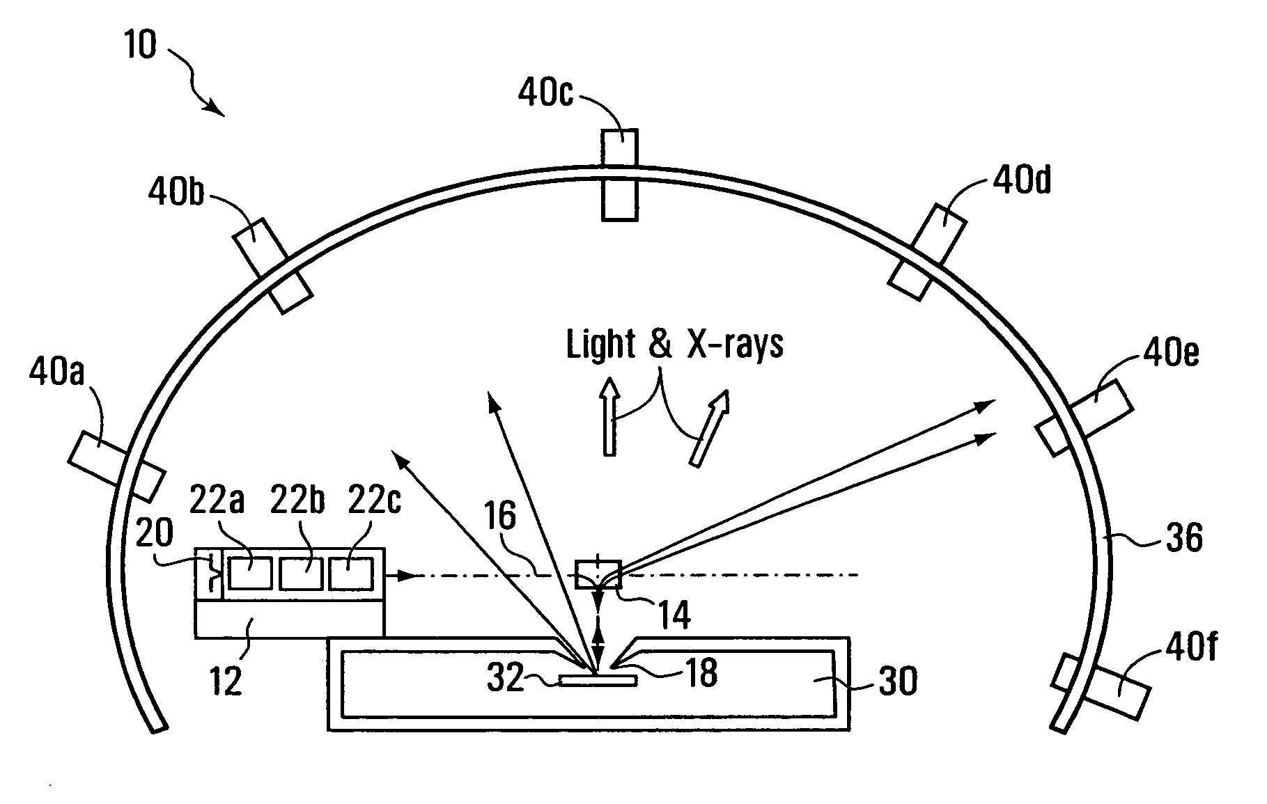
[0028] SEM 10, exemplary of an embodiment of the present invention, is schematically depicted in FIG. 1. SEM 10 includes an SEM column 12, placed on its side, and a magnetic separator 14. Magnetic separator 14 guides an electron beam 16 emitted by SEM column 12, to change its direction of travel from generally horizontal to generally vertical. A primary electron beam 16 is directed by magnetic separator 14, through an objective lens 18 onto a specimen 32. In the depicted embodiment objective lens 18 forms part of a combined collection chamber / objective lens 30.

[0029] SEM column 12 includes conventional SEM components, and includes an electron gun 20, a series of electromagnetic lenses 22a, 22b, 22c (collectively lenses 22), scanning coils, stigmators, (not specifically illustrated) and the like. However, final lens 22c is no longer the objective lens of the microscope. Instead, the final lens 22c of SEM column 12 is used as an auxiliary lens whose main purpose is to focus beam 16 o...


PUM

PropertyMeasurementUnit
angleaaaaaaaaaa
anglesaaaaaaaaaa
angleaaaaaaaaaa

Abstract

In a scanning electron microscope, an emitted primary electron beam is diverted by an angle of at least about 45 degrees prior to incidence with a specimen. The beam may be bent by a magnetic separator. The separator may also serve to deflect secondary electron and back scattered electrons. As the angle of emissions and reflections from the specimen is close to the angle of incidence, bending the primary electron beam prior to incidence, allows the electron source to be located so as not to obstruct the travel of emissions and reflections to suitable detectors.

Description

CROSS-REFERENCE TO RELATED APPLICATIONS [0001] This application claims benefits from U.S. Provisional Patent Application No. 60 / 579,676 filed Jun. 16, 2004, the contents of which are hereby incorporated herein by reference.FIELD OF THE INVENTION [0002] The present invention relates generally to scanning electron microscopes (SEMs), and more particularly to SEMs in which a primary electron beam is deflected prior to incidence with a specimen. BACKGROUND OF THE INVENTION [0003] Scanning electron microscopes are highly versatile electron beam instruments that can provide images over 100 times more magnified than commercial optical microscopes. They have applications in a wide range of different research areas, including, medicine, biology, material science and microelectronics. [0004] In principle, many analytical techniques can be combined with the normal operation of a SEM, but in practice, they are limited to a few routinely used add-on attachments. The main reason for this lies in ...

Claims


Application Information

Patent Timeline
Patent Type & Authority Applications(United States)
IPC IPC(8): G01N23/00
CPCG01N23/225H01J37/256H01J37/28H01J2237/14H01J2237/24485H01J2237/2445H01J2237/2446H01J2237/24475H01J2237/2448H01J2237/24415
Inventor KHURSHEED, ANJAM
Owner NAT UNIV OF SINGAPORE
Why Eureka
Try Eureka