
Full-color organic light emitting display and method of fabricating the same

a technology of organic light and display device, which is applied in the direction of discharge tube luminescnet screen, discharge tube/lamp details, incadescent envelope/vessel, etc., can solve the problems of long time for white balance after oled drive, difficult to fabricate high-resolution display device, and structure deterioration quickly, so as to achieve less expensive and less complicated effect of manufacturing

Active Publication Date: 2006-03-23
SAMSUNG DISPLAY CO LTD
View PDF16 Cites 43 Cited by
  • Summary
  • Abstract
  • Description
  • Claims
  • Application Information

AI Technical Summary

Benefits of technology

[0012] It is further an object of the present invention to provide a method of making the OLED having the emission layer protected from moisture and oxygen.
[0013] It is yet an object of the present invention to provide a method of making the novel OLED that is less expensive and less complicated to make.
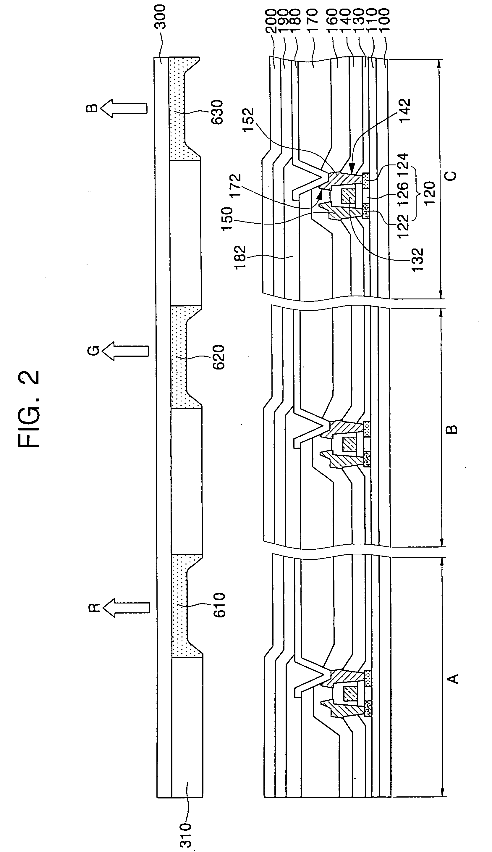
[0014] These and other objects can be achieved by a full-color OLED and method of fabricating the same, in which a moisture absorbent material and either color change mediums or color filter layers are formed on an encapsulation substrate, thus facilitating alignment during an encapsulation process and resulting in high-resolution OLEDs.

Problems solved by technology

However, since the respective emission layers corresponding to red (R), green (G), and blue (B) colors have life spans different from one another, it is difficult to keep white balance after the OLED is driven for a long time.
In addition, because of a technical limit for forming fine patterns in each pixel, it is difficult to fabricate high-resolution display devices.
However, I have found that such a structure deteriorates quickly because moisture and oxygen tend to destroy the emission layer.

Method used


Image

  • Full-color organic light emitting display and method of fabricating the same
  • Full-color organic light emitting display and method of fabricating the same
  • Full-color organic light emitting display and method of fabricating the same

Examples


Embodiment Construction

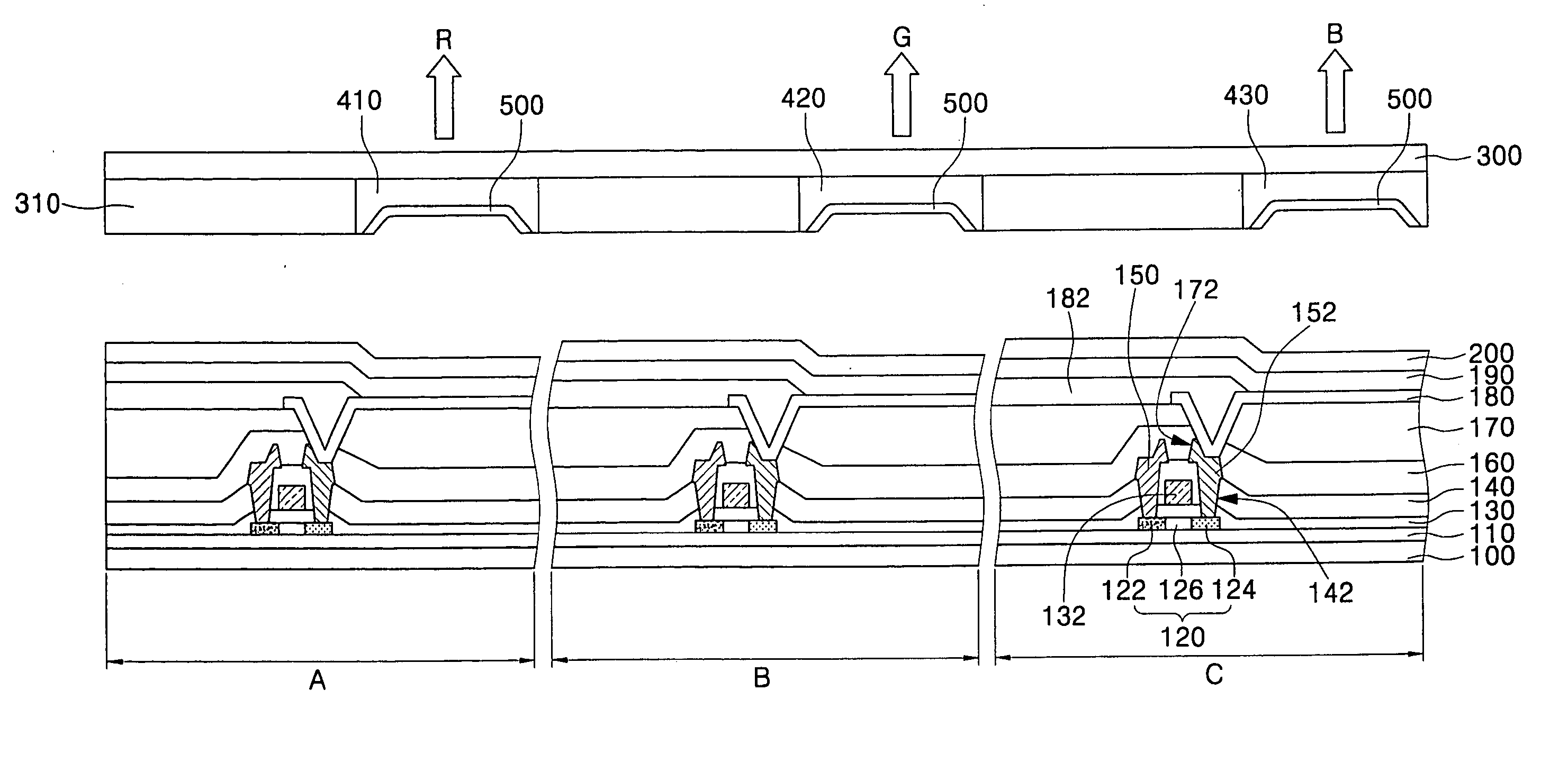
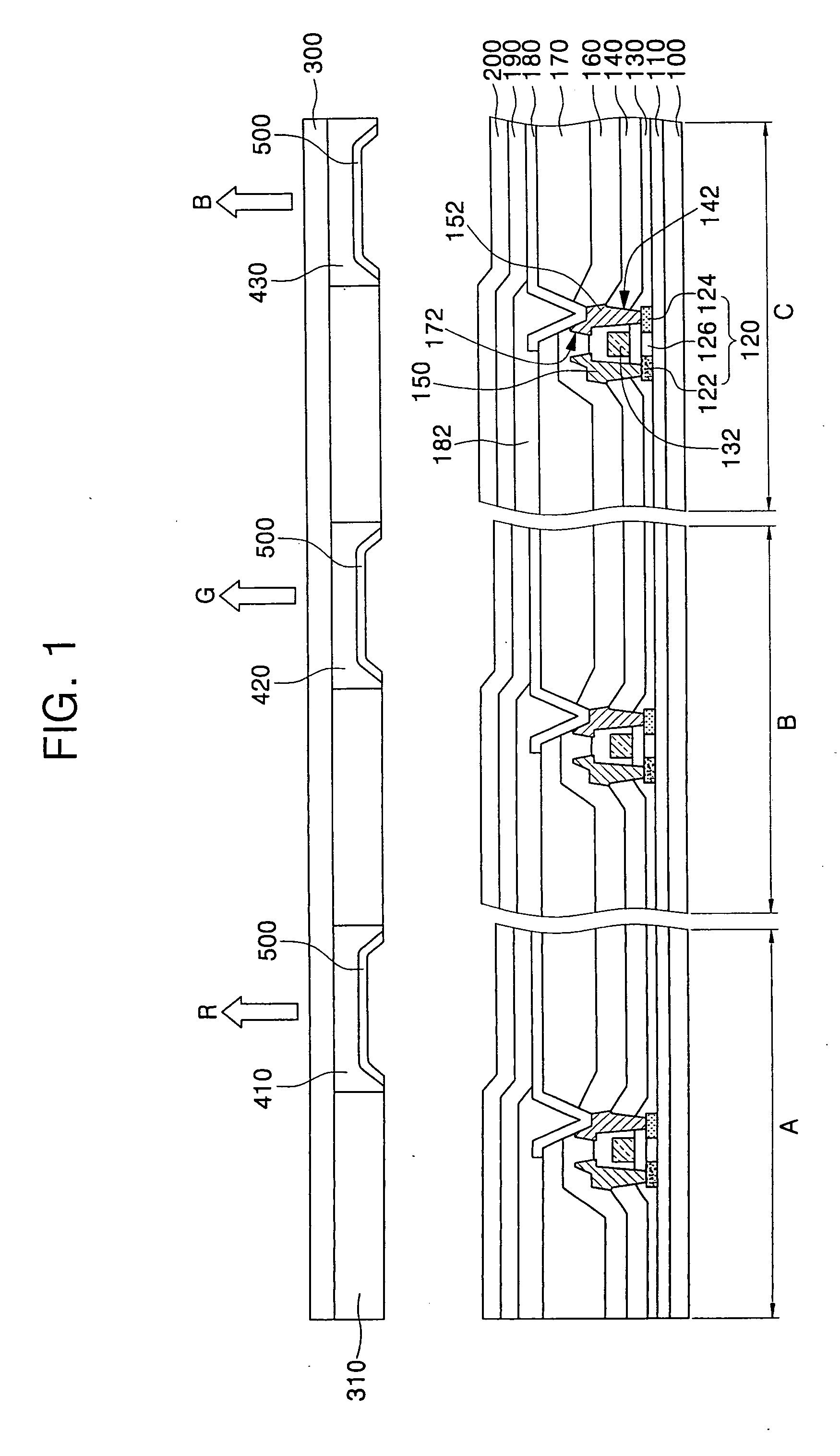
[0020] Turning now to FIG. 1, FIG. 1 is a schematic cross-sectional view of a full-color OLED according to an exemplary embodiment of the present invention. Referring to FIG. 1, the full-color OLED includes a substrate 100 and an encapsulation substrate 300. The substrate 100 includes a thin-film transistor (TFT) formed thereon. On substrate 100 is a gate electrode 132, a source electrode 150, a drain electrode 152, a pixel electrode 180 that is connected to any one of the source and drain electrodes 150 and 152, an organic emission layer 190 and an opposite electrode 200. The organic emission layer 190 and the opposite electrode 200 are disposed on top of the pixel electrode 180.

[0021] On the encapsulation substrate 300 of the OLED of FIG. 1 are color modification layers 410, 420 and 430. The color modification layers 410, 420 and 430 can be one of color filter layers or a color change mediums. The color modification layers 410, 420 and 430 also include moisture absorbent material...


PUM


Abstract

A full-color organic light emitting display (OLED) and method of fabricating the same. The display includes a substrate with a pixel electrode, an organic layer having at least an emission layer, and an opposite electrode formed thereon. An encapsulation substrate has formed thereon an organic emission layer that emits light of a single color and a black matrix that defines emission regions. A moisture absorbent material and one of color filter layers and color change mediums are formed between the black matrixes to correspond to the emission layer. The method of making alleviates the need for a separate processes for treating the moisture absorbent material and for forming the color filter layers or the color change mediums using a shadow mask.

Description

CLAIM OF PRIORITY [0001] This application makes reference to, incorporates the same herein, and claims all benefits accruing under 35 U.S.C. § 119 from an application for FULL COLOR OLED AND FABRICATING METHOD OF THE SAME earlier filed in the Korean Intellectual Property Office on 21 Sep. 2004 and there duly assigned Serial No. 2004-75642. BACKGROUND OF THE INVENTION [0002] 1. Field of the Invention [0003] The present invention relates to a full-color organic light emitting display (OLED) and method of fabricating the same, the display having an encapsulation substrate that includes a color modification layer having moisture absorbent materials, the color modification layer being either a color filter layer or a color change medium. [0004] 2. Description of the Related Art [0005] In general, an OLED includes a substrate, an anode disposed on the substrate, an emission layer disposed on the anode, a cathode disposed on the emission layer, and an encapsulation substrate. In such an OL...

Claims


Application Information

Patent Timeline
IPC IPC(8): H01L51/50H05B33/00
CPCH01L27/322H01L27/3244H01L51/56H01L51/5284H01L51/5237H10K59/38H10K59/12H10K2102/3026H10K59/874H10K59/123H10K71/421H10K59/8792H05B33/04H05B33/10H05B33/22H10K50/846H10K50/865H10K71/00
Inventor PARK, JOON-YOUNGKWON, JANG-HYUK
Owner SAMSUNG DISPLAY CO LTD
Learn More