
Semiconductor scheme for reduced circuit area in a simplified process

a simplified process and semiconductor technology, applied in the direction of semiconductor devices, semiconductor/solid-state device details, electrical devices, etc., can solve the problems of large computing power, reduced physical chip size, complicated design and fabrication processes, etc., to achieve less design space and efficiently measure alignment and bias

Inactive Publication Date: 2006-03-23
IBM CORP
View PDF9 Cites 2 Cited by
  • Summary
  • Abstract
  • Description
  • Claims
  • Application Information

AI Technical Summary

Benefits of technology

[0020] The present invention offers numerous advantages over conventional semiconductor schemes. For example, embodiments of the present invention require less design space and provide design engineers with alternative methods of interconnection for microelectronic devices. Embodiments of the present invention can also be used to more efficiently measure alignment and bias present in a microelectronic device. These and other features, aspects, and advantages will become better understood with reference to the following description, appended claims, and accompanying drawings.

Problems solved by technology

However, increasingly complex problems have demanded larger amounts of computing power, and as a result, more microelectronic devices such as field effect transistors (FETs) are needed to perform the necessary computations.
Moreover, while the demand for computing power has increased the transistor counts on computer chips, physical chip size has been reduced or held constant thus complicating design and fabrication processes.
The methods known are expensive processes that require a significant number of steps and generally require over a month to complete.
The alignment process is never perfect; however, the overlay alignment measurement is critical for FET operation and must be tightly and measurably controlled during manufacture.
Currently, there is no accurate measurement of this important parameter that can be done effectively and at low cost.
Metal interconnection uses up valuable space that is needed to interconnect logical blocks on the semiconductor chip.
Controlling precision in the etching process is a difficult task, and also requires that an additional etching step be inserted into the transistor fabrication process requiring more time and additional etching materials expenses.
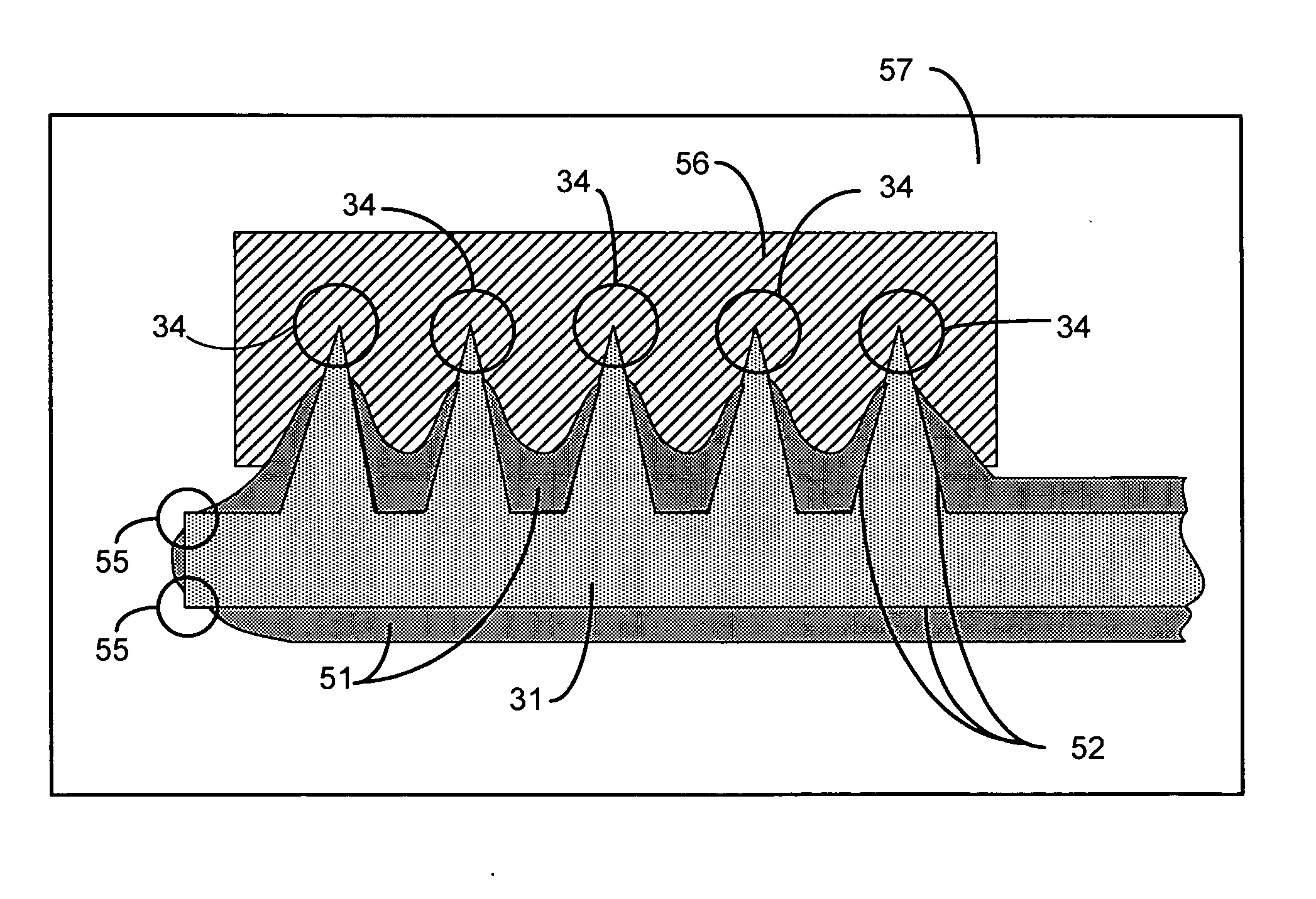
Also, it is presently not desirable and considered a groundrule design violation to form a polysilicon shape containing a small angle such that when a spacer is formed on a polysilicon shape, a portion of a vertical surface of the polysilicon shape becomes silicided and can become shorted to the silicon area.
If such a design were permitted to exist in the current state of the art, FET designs would not function as designed due to shorts that would occur between the exposed polysilicon and the silicon area.

Method used


Image

  • Semiconductor scheme for reduced circuit area in a simplified process
  • Semiconductor scheme for reduced circuit area in a simplified process
  • Semiconductor scheme for reduced circuit area in a simplified process

Examples


case 3

[0058] Case 3 of FIG. 11 (illustrated in FIG. 12C) is an embodiment displaying both misalignment and bias. Bias can be inferred by the presence of 16 shorts indicating the silicon area has increased in size by 4 grid points. Examining the numerical open / short representation for polysilicon shapes on the left side, it could be inferred that the polysilicon shape pairs are shifted to right five grid points; however, the numerical open / short sequence in Column C indicates the right side is shifted to the right by one grid point. To resolve the alignment discrepancy of each side, the surplus of shorts is averaged between the two sides and the correct measurement of misalignment is three grid points to the right. Case 4 of FIG. 11 illustrates an unusable product or faulty test. The random occurrences of shorts and opens reveal faulty fabrication, damage to the device, or some other event rendering the device useless. Bias and misalignment cannot be measured based on such results.

[0059] T...


PUM


Abstract

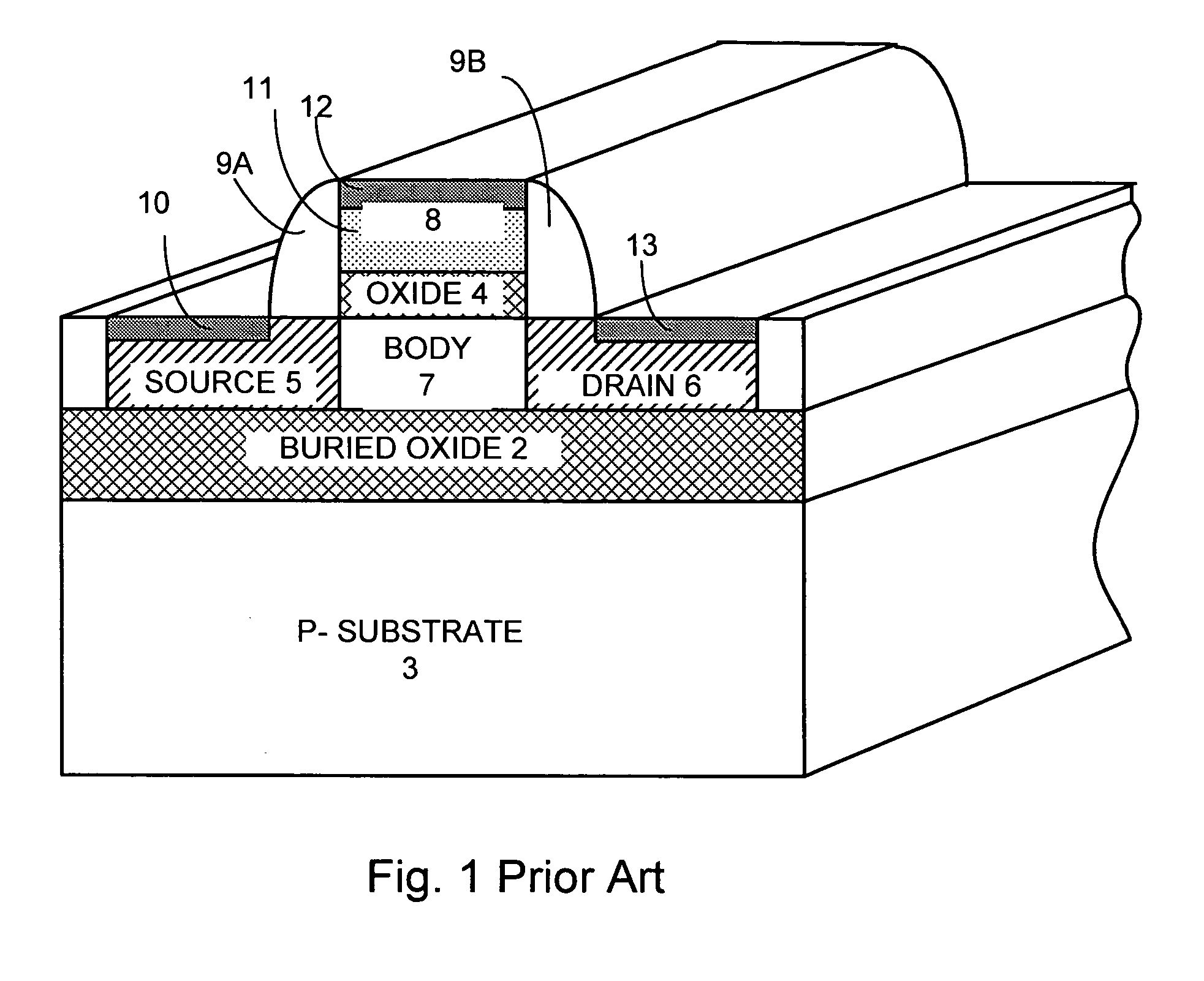
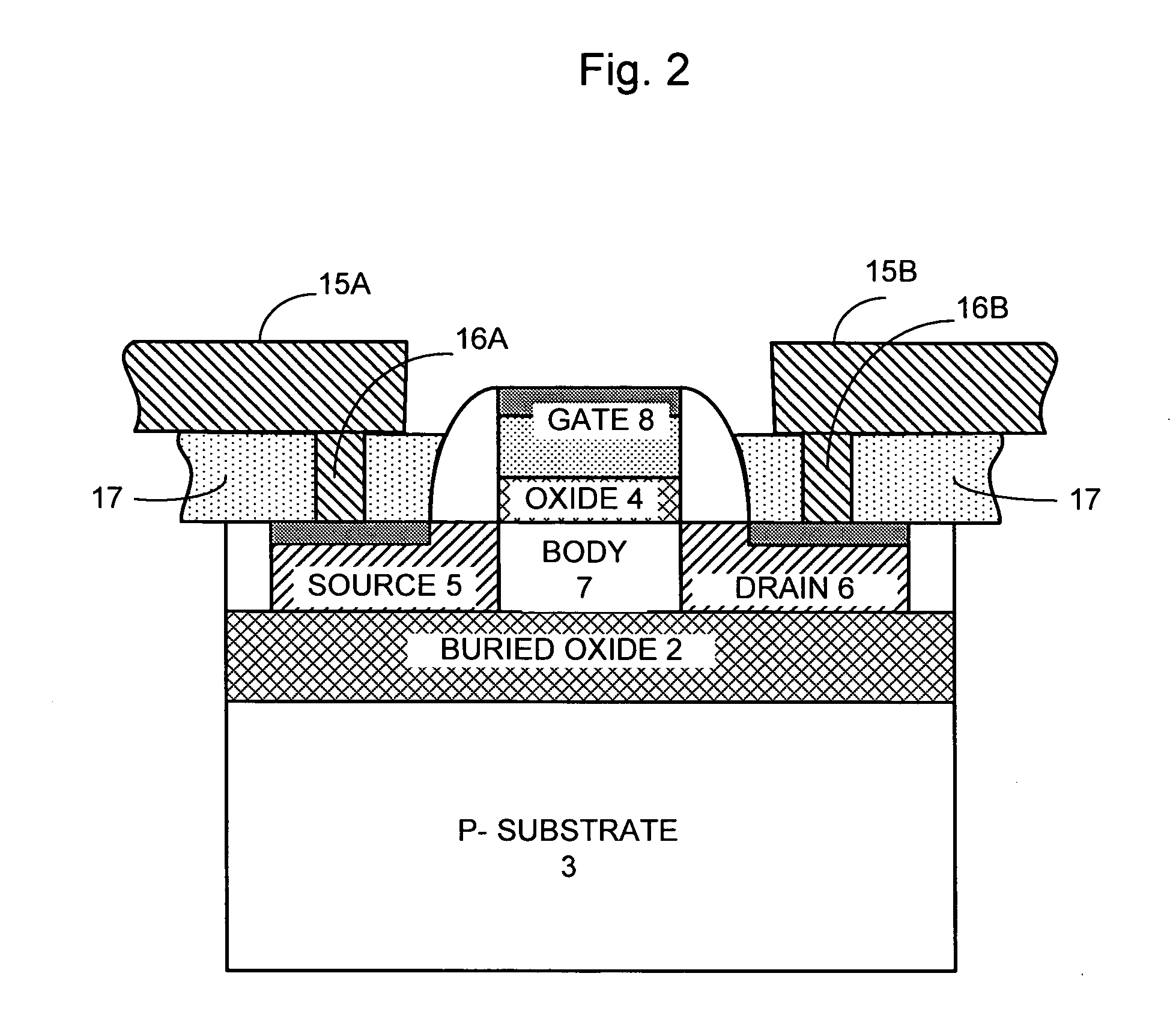
An apparatus and method are disclosed for an improved semiconductor interconnect scheme using a simplified process. In an embodiment of the apparatus, a polysilicon shape is formed on a silicon area. The polysilicon shape is created having a bridging vertex. When a spacer is created on the polysilicon shape, the spacer width is formed to be small enough near the bridging vertex to allow a silicide bridge to form that creates an electrical coupling between the silicon area and the bridging vertex. Semiconductor devices and circuits are created using the improved semiconductor interconnect scheme using the simplified process.

Description

CROSS-REFERENCE TO RELATED APPLICATIONS [0001] This application contains subject matter which is related to the subject matter of the commonly owned, co-pending U.S. Application entitled “Electrical Open / Short Contact Alignment Structure for Active Region vs. Gate Region”, filed concurrently, and having attorney docket number ROC920040275US1, hereby incorporated herein by reference in its entirety.BACKGROUND OF THE INVENTION [0002] 1. Field of the Invention [0003] The current invention generally relates to integrated circuit design and fabrication. More specifically, the current invention relates to silicide semiconductor production processes. [0004] 2. Description of the Related Art [0005] Continuous improvements in the design and fabrication of microelectronic devices have led to smaller and faster computing devices capable of solving increasingly complex problems. Rapid gains in the performance of these devices have enabled technology users to solve increasingly complex problems....

Claims


Application Information

Patent Timeline
Patent Type & Authority Applications(United States)
IPC IPC(8): H01L29/40H01L21/44
CPCH01L21/28518H01L21/76889H01L29/785H01L29/458H01L21/76895
Inventor CHRISTENSEN, TODD ALANDONZE, RICHARD LEEHOVIS, WILLIAM PAULKUEPER, TERRANCE WAYNESHEETS, JOHN EDWARD II
Owner IBM CORP
Learn More