Display unit, drive circuit, amorphous silicon thin-film transistor, and method of driving OLED

Inactive Publication Date: 2006-03-23
IBM CORP
View PDF4 Cites 12 Cited by
  • Summary
  • Abstract
  • Description
  • Claims
  • Application Information

AI Technical Summary

Benefits of technology

[0025] An amorphous silicon thin-film transistor to which the present invention is applied is characterized by including a gate electrode, amorphous silicon, a source electrode and a drain electrode which face the gate electrode with the amorphous silicon interposed therebetween, and a twig electrode formed by separating a portion of one of the source electrode and the drain electrode, and characterized i

Problems solved by technology

This OLED is a current-driven device, and a reduction in image quality results directly from variations in drive transistors for driving the OLEDs or variations in current due to degradation.
However, if the OLED 200 is driven by using an amorphous silicon (a-Si) thin-film transistor (TFT) for example, and if there is a need to cause a sufficiently large current to flow thr

Method used


Image

  • Display unit, drive circuit, amorphous silicon thin-film transistor, and method of driving OLED
  • Display unit, drive circuit, amorphous silicon thin-film transistor, and method of driving OLED
  • Display unit, drive circuit, amorphous silicon thin-film transistor, and method of driving OLED

Examples


Example

[0037] The present invention will be described in detail with respect to an embodiment thereof with reference to the accompanying drawings.

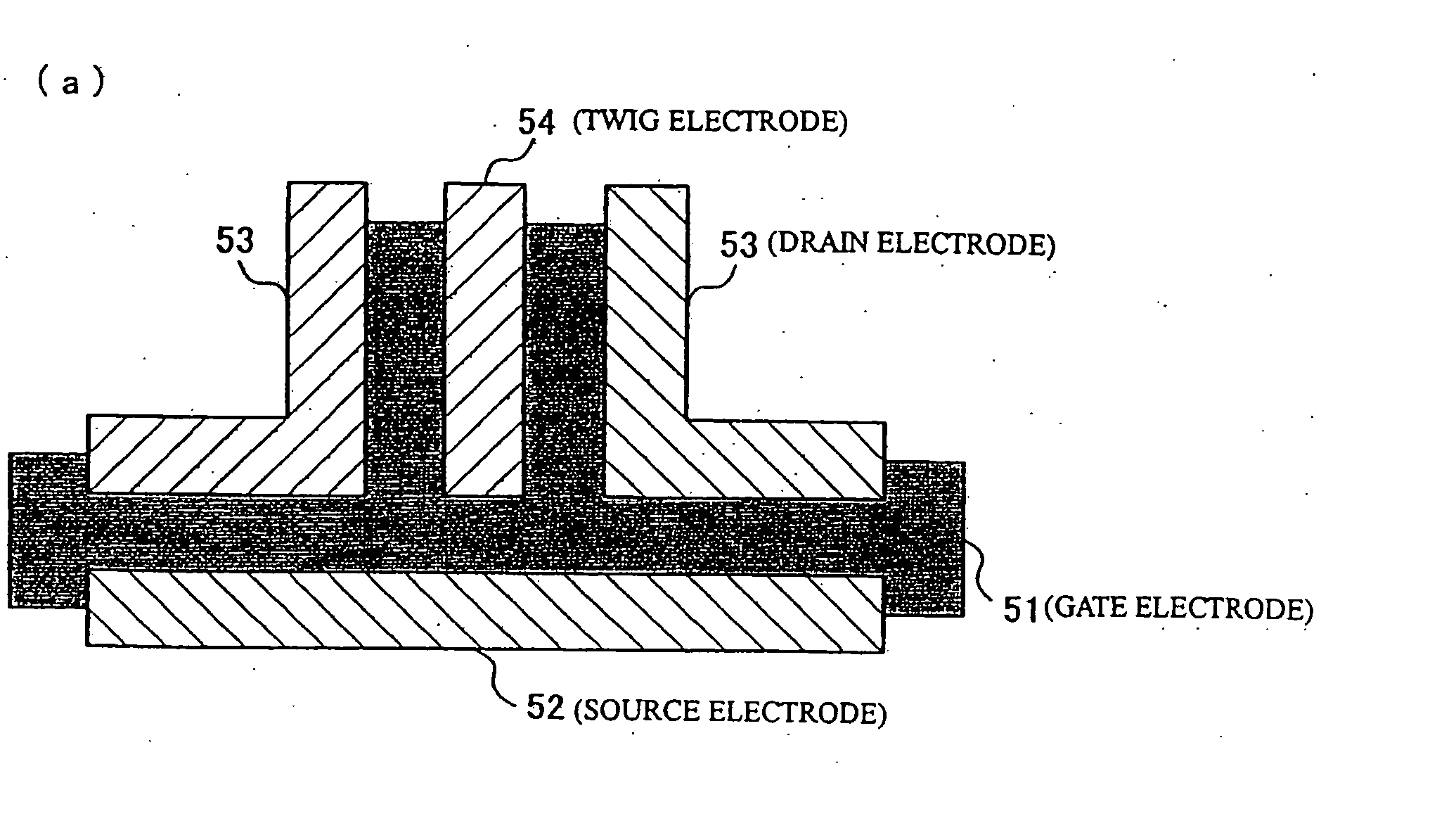
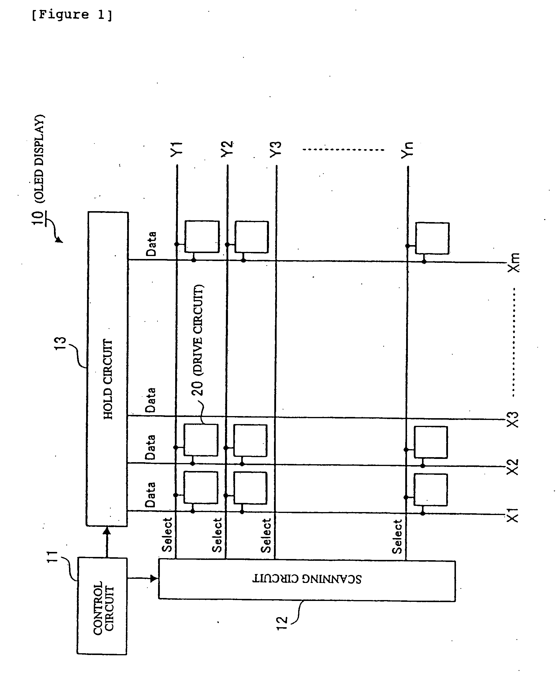
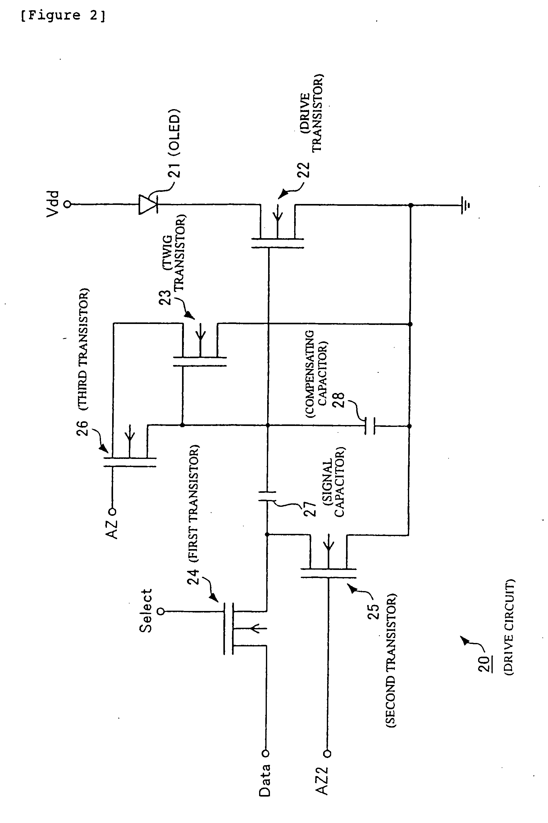
[0038] Description of symbols [0039]10 . . . OLED display [0040]11 . . . Control circuit [0041]12 . . . Scanning circuit [0042]13 . . . Hold circuit [0043]20 . . . Drive circuit [0044]21 . . . Organic light emitting diode (OLED) [0045]22 . . . Drive transistor [0046]23 . . . Twig transistor [0047]24 . . . First transistor [0048]25 . . . Second transistor [0049]26 . . . Third transistor [0050]27 . . . Signal capacitor [0051]28 . . . Compensating capacitor [0052]31 . . . OLED [0053]32 . . . Drive transistor [0054]33 . . . Twig transistor [0055]34 . . . First transistor [0056]35 . . . Second transistor [0057]36 . . . Third transistor [0058]37 . . . Fourth transistor [0059]38 . . . Signal capacitor [0060]39 . . . Compensating capacitor [0061]51 . . . Gate electrode [0062]52 . . . Source electrode [0063]53 . . . Drain electrode [0064]54 . . . Twig el...


PUM


Abstract

A display unit has an organic light emitting diode (OLED) 21 provided in correspondence with each of pixels and capable of emitting light by itself, a drive transistor 22 for driving the OLED 21, a twig transistor 23 which is formed so as to have a portion of an electrode of the drive transistor 22 independently formed, and which is used to detect a threshold voltage (Vth) of the drive transistor 22, a compensating capacitor 28 in which the threshold voltage (Vth) detected by the twig transistor 23 is written, a signal capacitor 27 in which a signal voltage to be supplied to the drive transistor 22 is written, a first transistor 24 provided between a data line and the signal capacitor 27, a second transistor 25 provided between the signal capacitor 27 and the compensating capacitor 28, and a third transistor 26 provided between a gate electrode and another electrode of the twig transistor 23.

Description

BACKGROUND OF THE INVENTION [0001] 1. Field of the Invention [0002] The present invention relates to a display unit or the like using an organic light emitting diode (OLED). More particularly, the present invention relates to a display unit or the like in which compensation is made for variation in the threshold voltage (Vth) of a drive transistor. [0003] 2. Discussion of the Prior Art [0004] An OLED (also referred to as “organic EL”) is a device in which a dc voltage is applied to a fluorescent organic compound capable of being excited in an electric field to cause the compound to emit light, and which attracts attention as a next-generation display device. This OLED is a current-driven device, and a reduction in image quality results directly from variations in drive transistors for driving the OLEDs or variations in current due to degradation. In improving the image quality, it is effective to use a method of stabilizing the current output from each drive transistor by making com...

Claims


Application Information

Patent Timeline
IPC IPC(8): G09G3/10G09G3/36G09F9/30G09G3/20H01L51/50G09G3/30G09G3/32G09G3/3225G09G3/3266G09G3/3283G09G3/3291H01L27/32H01L29/417H01L29/423H01L29/786
CPCG09G3/3233G09G3/325G09G2300/0426G09G2300/0819G09G2300/0842H01L29/78669G09G2310/06G09G2320/043H01L27/3244H01L29/41733H01L29/42384G09G2300/0861H10K59/12
Inventor KOBAYASHI, YOSHINAOTSUJIMURA, TAKATOSHIONO, SHINYA
Owner IBM CORP
Why Eureka
Try Eureka