Solid-state image pickup device and driving method thereof

a solid-state image and pickup device technology, applied in the direction of color television, television system, radio control device, etc., can solve the problem that the substrate modulation type sensor cannot be miniaturized

Inactive Publication Date: 2006-03-23
SEIKO EPSON CORP
View PDF10 Cites 7 Cited by
  • Summary
  • Abstract
  • Description
  • Claims
  • Application Information

AI Technical Summary

Benefits of technology

[0007] An advantage of the present invention is to provide a solid-state image pickup device that can realize miniaturization of the substrate modulation type sensor by narrowing the cell pitch of the substrate modulation type sensor.
[0008] According to an aspect of the invention, a solid-state image pickup device having inside a substrate a plurality of accumulation wells that accumulate light-producing electric charge produced in a photoelectric conversion region corresponding to light applied thereto, the plurality of photoelectric conversion regions being arranged in a two-dimensional matrix on the substrate, includes: a plurality of modulation transistors, each of which is provided in every pair of the photoelectric conversion regions adjoined in one direction of the two-dimensional matrix, which control a threshold voltage of a channel using the light-producing electric charge held in a modulation well, and which output a pixel signal corresponding to the light-producing electric charge; a plurality of transfer control elements, each pair of which is provided in every pair of the adjoining photoelectric conversion regions, which shift a potential barrier of a path for transferring the light-producing electric charge between each accumulation well and the corresponding modulation well in the pair of photoelectric conversion regions, and which control the transfer of the light-producing electric charge; and a plurality of transfer gate lines coupled to each of the transfer control elements in the plurality of photoelectric conversion regions arranged in the other direction of the two-dimensional matrix; in that each gate of the plurality of modulation transistors is in a ring-like shape, each gate being provided in a manner that at least a portion of the gate is interposed between partially cut-off portions of every pair of the approximately rectangular photoelectric conversion regions adjoined in one direction of the two-dimensional.
[0009] With such a structure, it is possible to realize the solid-state image pickup device that enables miniaturization of the substrate modulation type sensor by narrowing the cell pitch of the substrate modulation type sensor.
[0010] According to another aspect of the invention, a method for driving the solid-state image pickup device having inside a substrate a plurality of accumulation wells that accumulate light-producing electric charge produced in a photoelectric conversion region corresponding to light applied thereto, the plurality of photoelectric conversion regions being arranged in a two-dimensional matrix on the substrate, contains: a plurality of modulation transistors, each of which is provided in every pair of the photoelectric conversion regions adjoined in one direction of the two-dimensional matrix, which control a threshold voltage of a channel using the light-producing electric charge held in a modulation well, and which output a pixel signal corresponding to the light-producing electric charge; a plurality of transfer control elements, each pair of which is provided in every pair of the adjoining photoelectric conversion regions, which shift a potential barrier of a path for transferring the light-producing electric charge between each accumulation well and the corresponding modulation well in the pair of photoelectric conversion regions, and which control the transfer of the light-producing electric charge; and a plurality of transfer gate lines coupled to each of the transfer control elements in the plurality of photoelectric conversion regions arranged in the other direction of the two-dimensional matrix. Each gate of the plurality of modulation transistors is in a ring-like shape, each gate being provided in a manner that at least a portion of the gate is interposed between partially cut-off portions of every pair of the approximately rectangular photoelectric conversion regions adjoined in one direction of the two-dimensional, includes: firstly reading out a noise component from the modulation transistor by controlling a voltage of the gate provided corresponding to the pair of photoelectric conversion regions in one direction of the matrix; transferring the light-producing electric charge from one of the two accumulation wells in the pair of photoelectric conversion regions to the modulation well in one direction of the matrix; and secondly reading out a signal component from the modulation transistor based on the transferred light-producing electric charge by controlling a voltage of the gate provided corresponding to the pair of photoelectric conversion regions in one direction of the matrix.
[0011] With such a structure, it is possible to realize the method for driving the solid-state image pickup device that enables miniaturization of the substrate modulation type sensor by narrowing the cell pitch of the substrate modulation type sensor.

Problems solved by technology

Therefore, there is a problem in which the substrate modulation type sensor cannot be miniaturized because the ring gate needs to have more than a certain extent of width.

Method used


Image

  • Solid-state image pickup device and driving method thereof
  • Solid-state image pickup device and driving method thereof
  • Solid-state image pickup device and driving method thereof

Examples


Embodiment Construction

[0020] An embodiment of the invention will now be described with reference to the accompanying drawings.

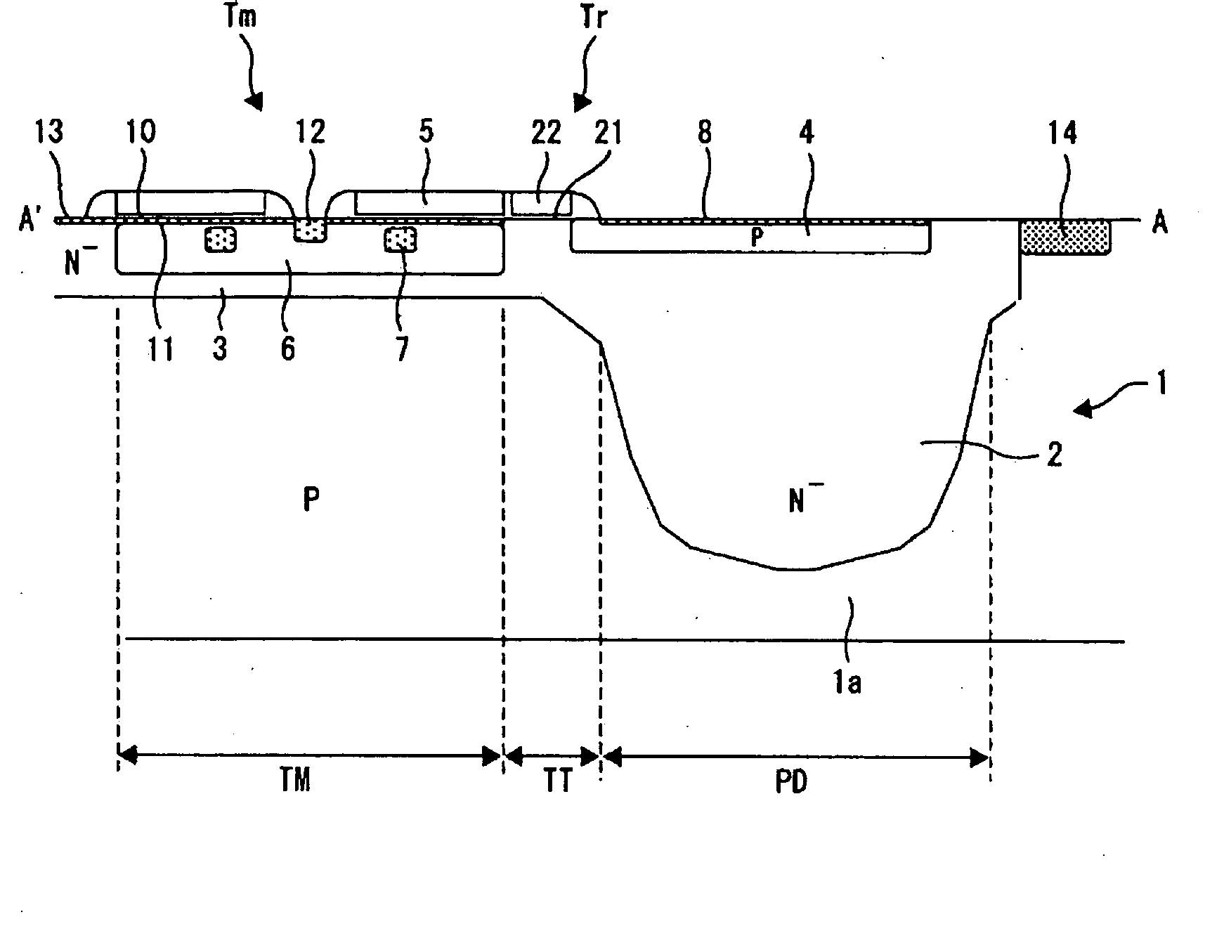
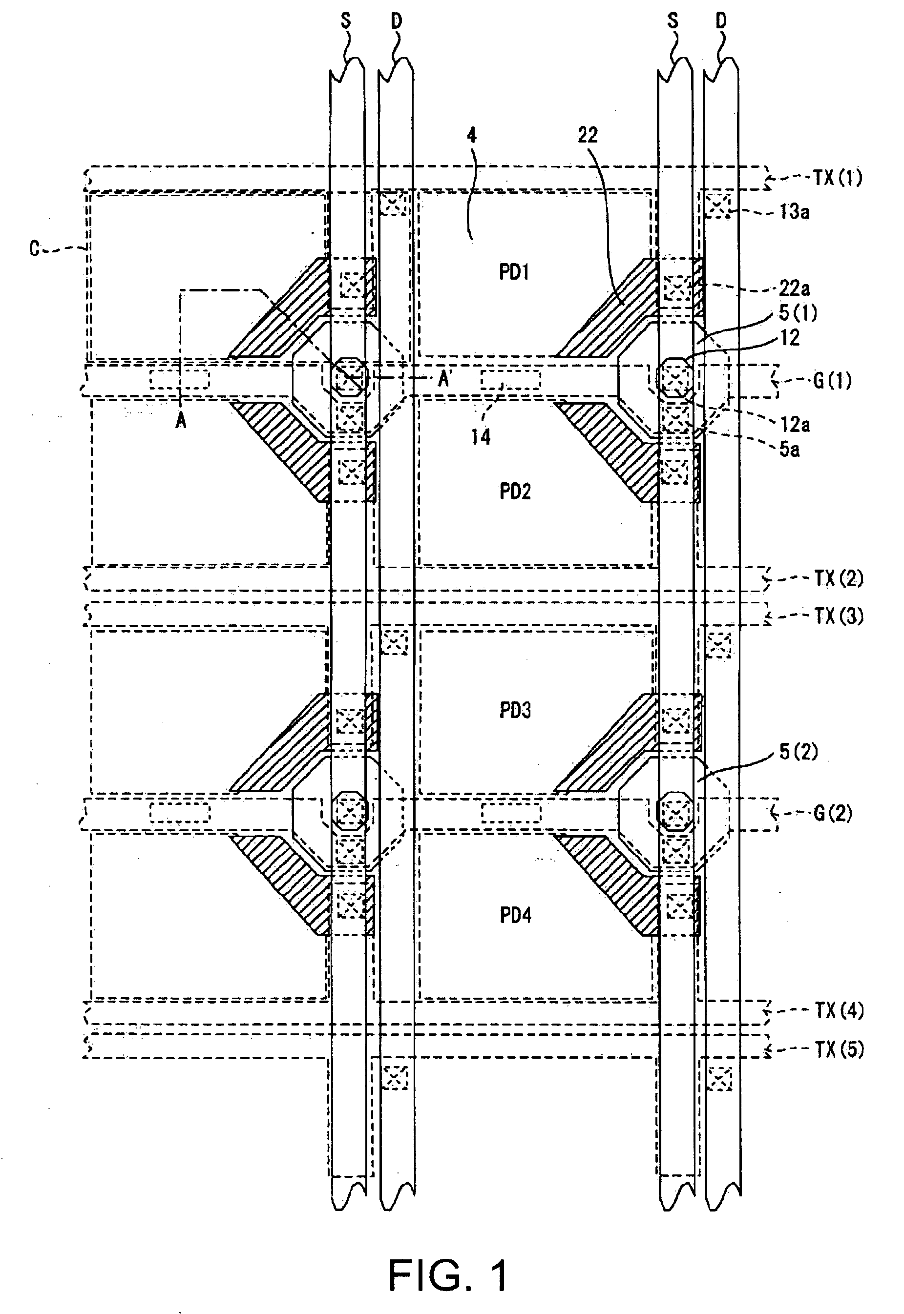
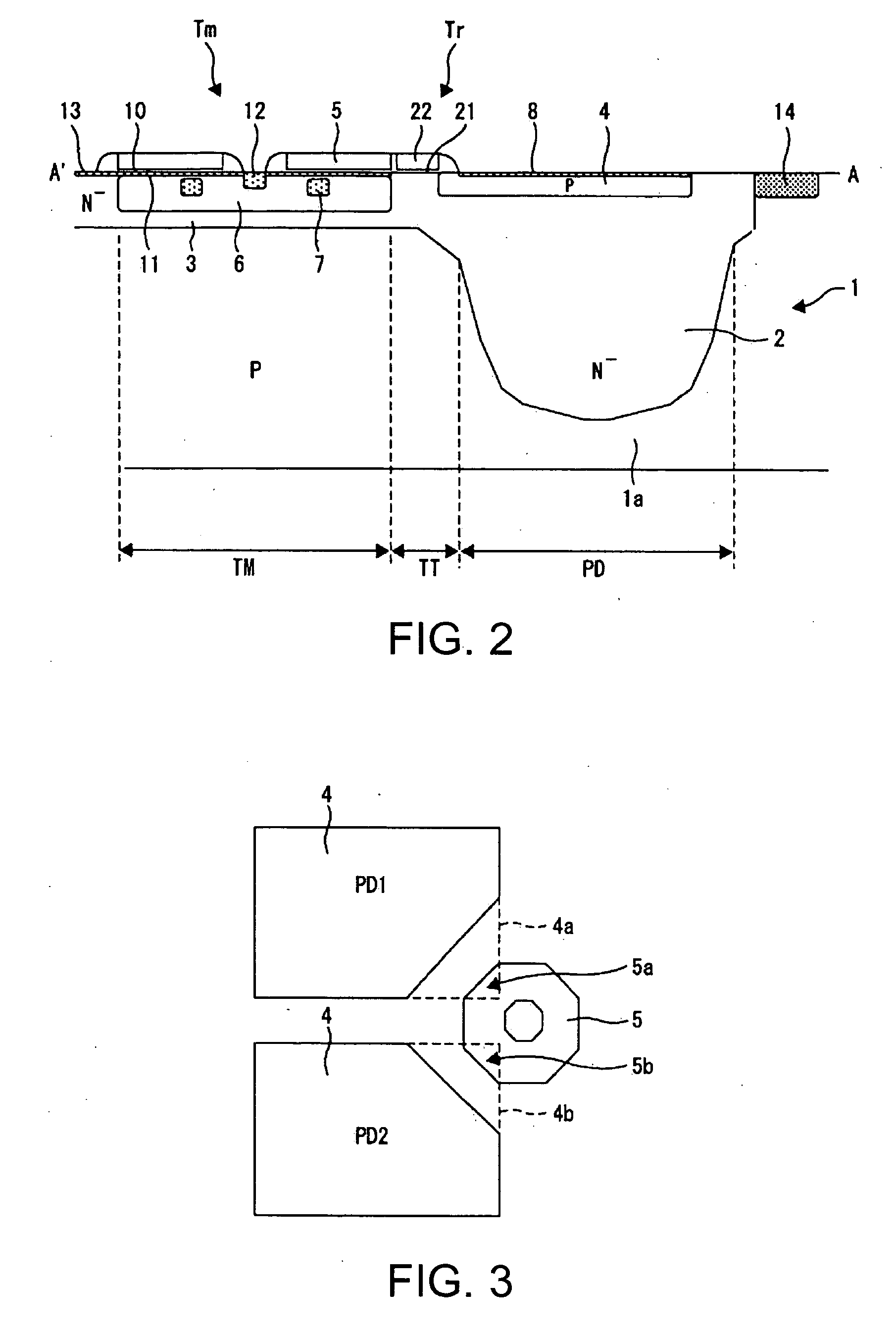
[0021] First, a structure of the solid-state image pickup device of the embodiment of the invention will be described. FIG. 1 is a plan view showing a planar configuration of a solid-state image pickup device according to the embodiment of the invention. FIG. 2 is a cross-sectional diagram taken along an A-A′ line of FIG. 1.

[0022] As shown in FIG. 1, the solid-state image pickup device of the embodiment is a censor cell array having a plurality of sensor cells arranged in a two-dimensional matrix on a flat surface of a substrate. Each sensor cell accumulates light-producing electric charge produced corresponding to incident light and outputs a pixel signal at a level based on the accumulated light-producing charge. The pixel signals for one image can be obtained by arranging the sensor cells in matrix. In FIG. 1, a region surrounded by dotted lines is a sensor cell C which is a ...


PUM


Abstract

A solid-state image pickup device having inside a substrate a plurality of accumulation wells that accumulate light-producing electric charge produced in a photoelectric conversion region corresponding to light applied thereto, the plurality of photoelectric conversion regions being arranged in a two-dimensional matrix on the substrate, including: a plurality of modulation transistors, each of which is provided in every pair of the photoelectric conversion regions adjoined in one direction of the two-dimensional matrix, which control a threshold voltage of a channel using the light-producing electric charge held in a modulation well, and which output a pixel signal corresponding to the light-producing electric charge; a plurality of transfer control elements, each pair of which is provided in every pair of the adjoining photoelectric conversion regions, which shift a potential barrier of a path for transferring the light-producing electric charge between each accumulation well and the corresponding modulation well in the pair of photoelectric conversion regions, and which control the transfer of the light-producing electric charge; and a plurality of transfer gate lines coupled to each of the transfer control elements in the plurality of photoelectric conversion regions arranged in the other direction of the two-dimensional matrix; in that each gate of the plurality of modulation transistors is in a ring-like shape, each gate being provided in a manner that at least a portion of the gate is interposed between partially cut-off portions of every pair of the approximately rectangular photoelectric conversion regions adjoined in one direction of the two-dimensional.

Description

BACKGROUND OF THE INVENTION [0001] 1. Technical Field [0002] The present invention relates to a solid-state image pickup device and a method for driving the same. [0003] 2. Related Art [0004] As a solid-state image pickup device mounted on a cellular phone, a digital camera, or the like, there are a charge-coupled-device (CCD) type image sensor (hereinafter referred to as a CCD sensor) and a CMOS type image sensor (hereinafter referred to as a CMOS sensor.) [0005] Further, in recent years, a MOS type solid-state image pickup device (hereinafter referred to as a substrate modulation type sensor) that enables both high image quality and low electric consumption using a threshold voltage modulation method has been proposed (e.g., Japanese Unexamined Patent Publication No. 2002-134729.) In case of the substrate modulation type sensor, a ring gate is used in a modulation transistor. Each of a plurality of sensor cells arranged on a substrate in a two-dimensional matrix includes one ring ...

Claims


Application Information

Patent Timeline
Patent Type & Authority Applications(United States)
IPC IPC(8): H01L21/00H01L27/146H01L31/10H04N5/335H04N5/357H04N5/369H04N5/374H04N5/376
CPCH01L27/14609H01L27/14601
Inventor KUWAZAWA, KAZUNOBU
Owner SEIKO EPSON CORP
Why Eureka
Try Eureka