
Wave interrogated near field arrays system and method for detection of subwavelength scale anomalies

a near field array and subwavelength scale technology, applied in the direction of instruments, semiconductor/solid-state device testing/measurement, nuclear engineering, etc., can solve the problems of affecting the accuracy of the detection method, and the inability to accurately detect the spot size. , to achieve the effect of retaining the convenience and speed of far-field scattering data collection

Inactive Publication Date: 2006-03-30
THE ARIZONA BOARD OF REGENTS ON BEHALF OF THE UNIV OF ARIZONA
View PDF1 Cites 42 Cited by
  • Summary
  • Abstract
  • Description
  • Claims
  • Application Information

AI Technical Summary

Benefits of technology

[0009] The present invention exploits the benefits of near-field energy concentration, while retaining the convenience and speed of far-field scattering data collection.

Problems solved by technology

This came, however, at the expense of a tremendous degradation in illumination, as a transmission efficiency of 10−5 was reported.
The techniques used in the prior art generally suffer from very small transmission efficiencies (i.e., the ratio of incident power to power at the tip) because the concentration of the wave energy is achieved by guiding the wave through closed waveguides that are well below cutoff.
A second issue left unaddressed, but which is critical to the application of defect detection on large semiconductor wafers, is that the minuteness of the spot-size implies an enormous scanning time as the illuminated region is physically moved over the area to be examined.

Method used


Image

  • Wave interrogated near field arrays system and method for detection of subwavelength scale anomalies
  • Wave interrogated near field arrays system and method for detection of subwavelength scale anomalies
  • Wave interrogated near field arrays system and method for detection of subwavelength scale anomalies

Examples


Embodiment Construction

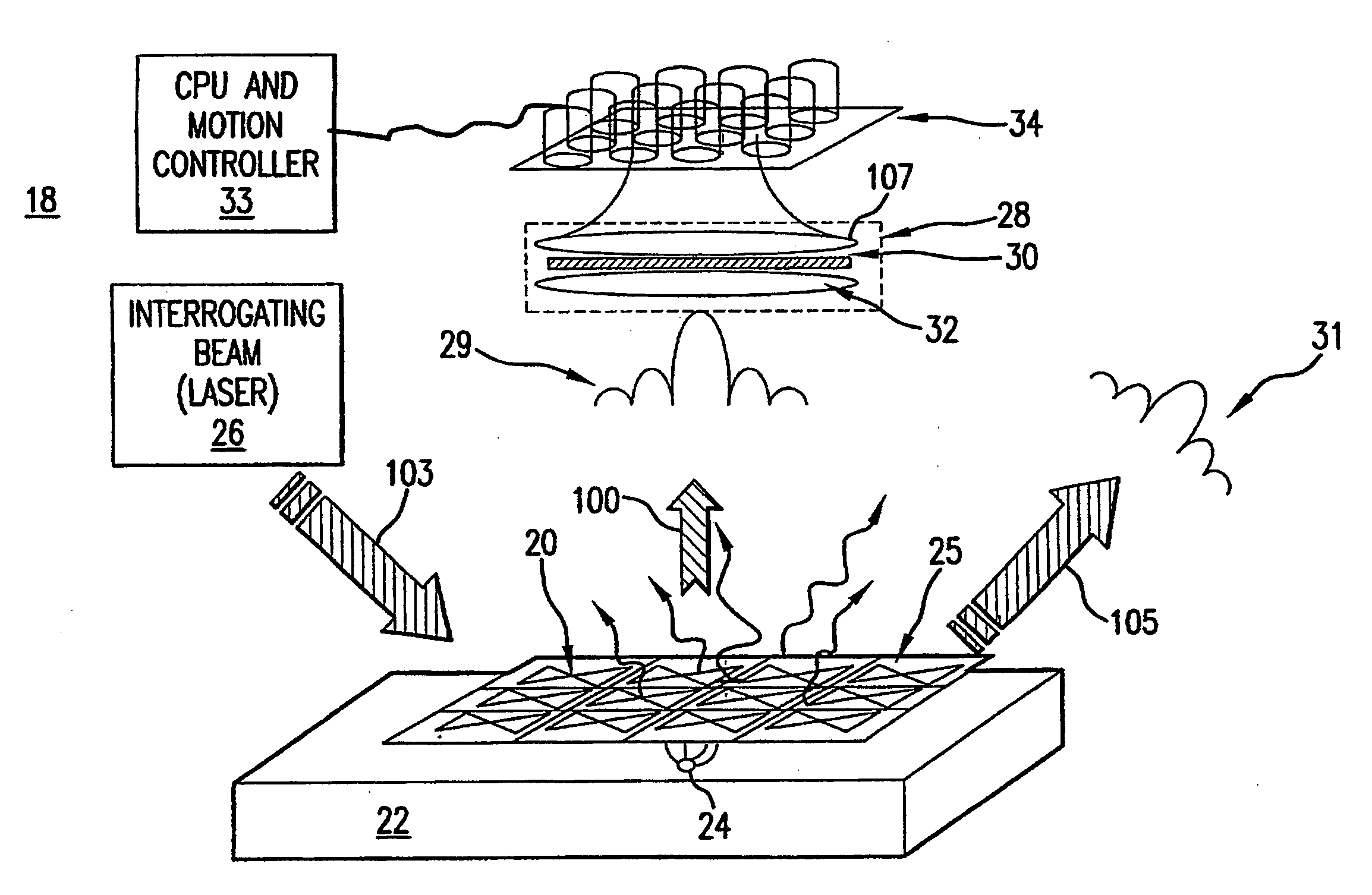
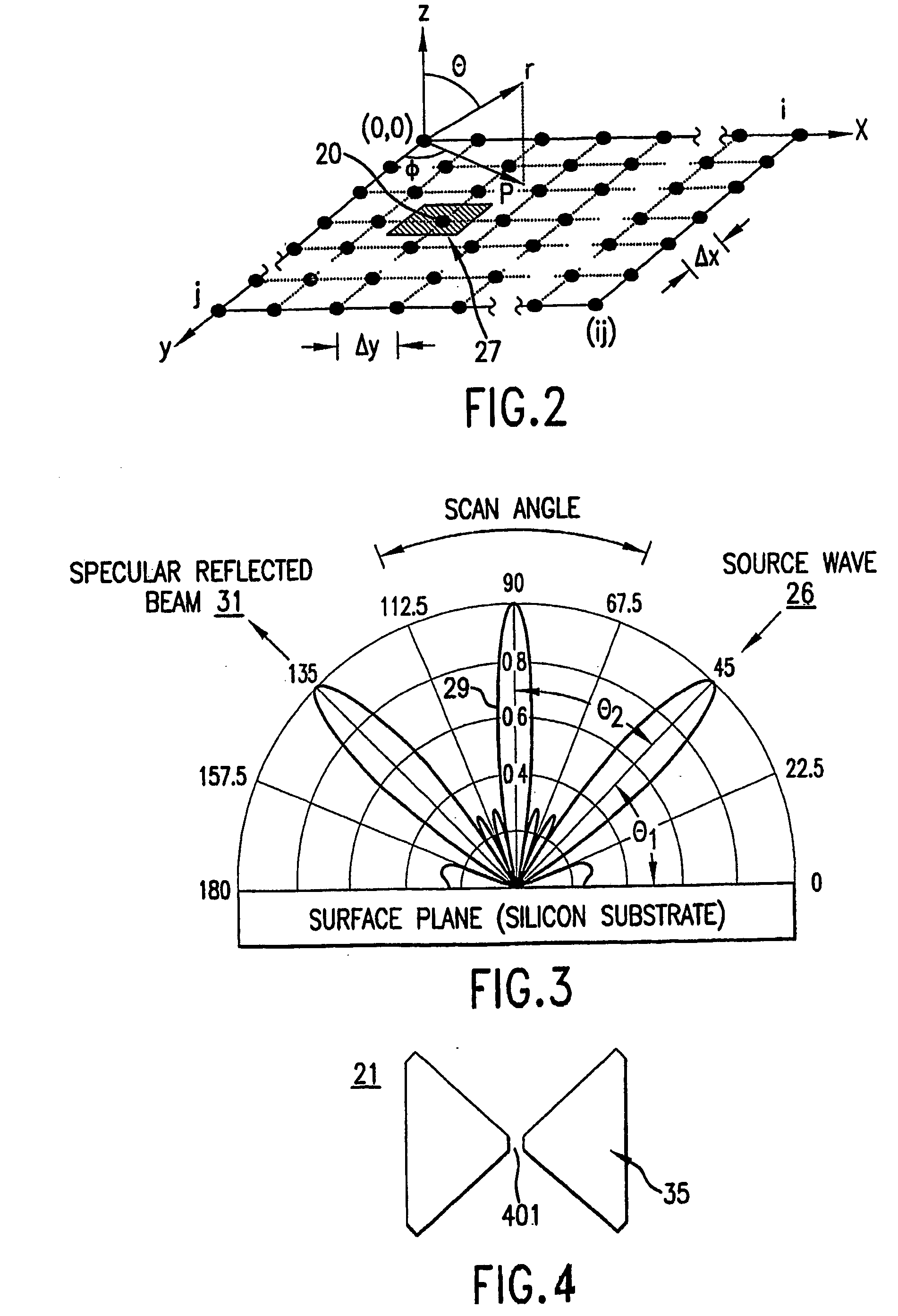
[0028]FIGS. 1-3 depict one exemplary embodiment of the present invention. A wave interrogated near field array system 18 is shown to include a plurality of antenna elements or probes 20, which may be constructed of open circuited bow-tie antennas on an optically transparent substrate 25. The transparent substrate 25 may be fabricated from SiO2, BK7, or other suitable optical glass. A substrate 22 to be examined for anomalies may be provided under the array of antenna elements 20. The substrate 22 may for instance be silicon, metallic, or magnetic media. The array typically is placed at a height of approximately 70 nm from the surface of the substrate 22 to be examined. The antenna elements 20 may be illuminated by a reference source 26, which may be coherent monochromatic source, for example a laser, emitting electromagnetic energy having a characteristic wavelength (λ), producing a free space wave. In one exemplary embodiment, the characteristic wavelength λ of the energy source is...


PUM


Abstract

An array of antenna elements (20) can be used to detect subwavelength sized anomalies on a surface below the array. An array (20) is illuminated at optical frequencies by a coherent optical energy source (26). The change in reactance and radiated power of the antenna elements that results from the proximity of the anomaly to the near field of the antenna element's open-circuited is detected and holographically filtered to eliminate the radiation caused by the antenna array itself. Image processing is performed on the detected scattered radiation (100) to determine whether an anomaly is present and to locate the anomaly and its characteristics.

Description

CROSS REFERENCE TO RELATED APPLICATION [0001] This application claims priority to provisional application Ser. No. 60 / 361,650 filed 5 Mar. 2002 entitled: “A HIGH SENSITIVITY ANTENNA ELEMENT FOR NEAR FIELD PROBE APPLICATIONS”, which is incorporated herein by reference in its entirety.BACKGROUND OF THE INVENTION [0002] 1. Field of the Invention [0003] In one aspect, this invention is a method and system for detecting sub-wavelength size anomalies in a substrate using optical radiation and an array of resonant photonic open feed antenna elements. In another aspect, this invention is directed to a closed flux resonant antenna that may be used in a system for detecting sub-wavelength size anomalies in a substrate. [0004] 2. Background Information [0005] On semiconductor substrates, anomalies, such as process contaminants, post-polishing substrate fragments, or voids need to be accurately located and identified in order to obtain the cleanliness required for the next generation of integra...

Claims


Application Information

Patent Timeline
IPC IPC(8): G01N21/86G01V8/00G01B11/30G01N21/47G01N21/94G01N21/95G01N21/958H01L21/66
CPCG01N21/47G01N21/9501G01N21/94
Inventor DIAZ, RODOLFO E.WATTS, MICHAEL
Owner THE ARIZONA BOARD OF REGENTS ON BEHALF OF THE UNIV OF ARIZONA
Learn More