Method for testing semiconductor devices and an apparatus therefor

a semiconductor device and apparatus technology, applied in the direction of individual semiconductor device testing, semiconductor/solid-state device testing/measurement, instruments, etc., can solve problems such as adverse effects on duts

Inactive Publication Date: 2006-03-30
KES SYST
View PDF23 Cites 49 Cited by
  • Summary
  • Abstract
  • Description
  • Claims
  • Application Information

AI Technical Summary

Benefits of technology

[0030] In the second mode, DUTs are not individually tested in the test plate. Rather the test board is populated with DUTs that are transferred from the input carrier tray to the precisor and then to the test board by the pick-and-place mechanism. Once the test board has been populated with DUTs by the pick-and-place mechanism, the test board is moved to the secon

Problems solved by technology

Although the DUTs will be packaged, it is still desirable for the DUTs to be protected

Method used


Image

  • Method for testing semiconductor devices and an apparatus therefor
  • Method for testing semiconductor devices and an apparatus therefor
  • Method for testing semiconductor devices and an apparatus therefor

Examples


Embodiment Construction

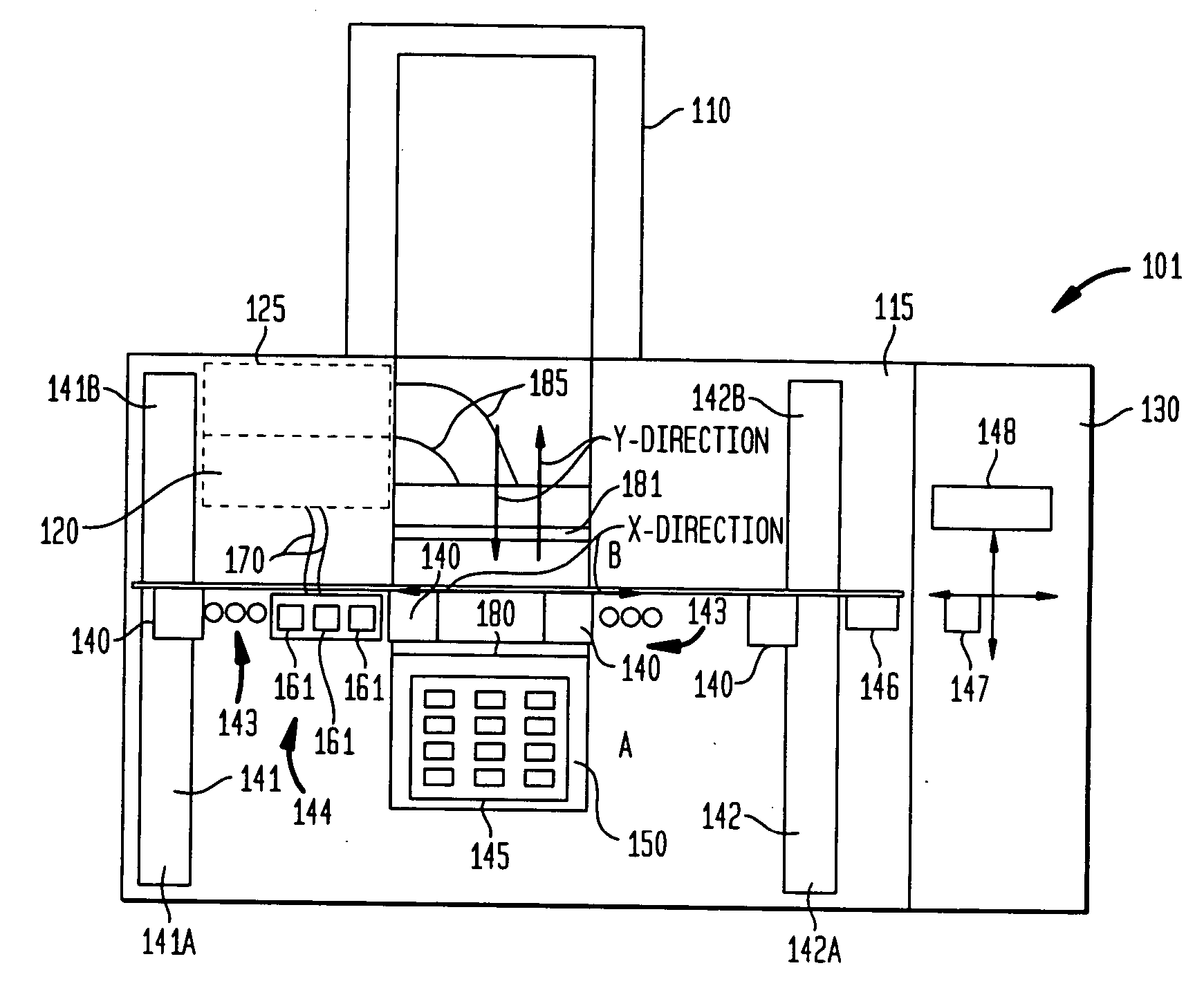
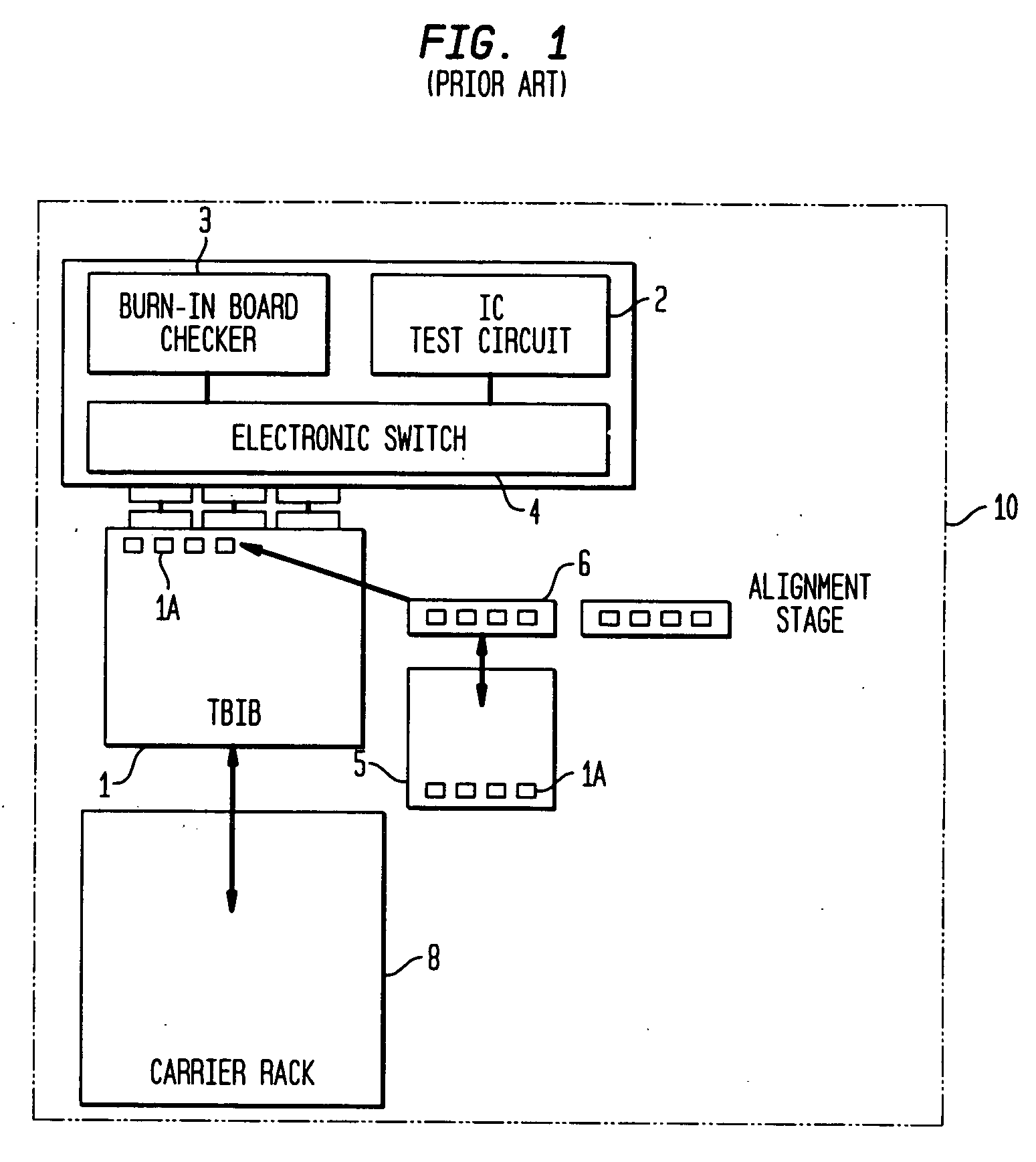
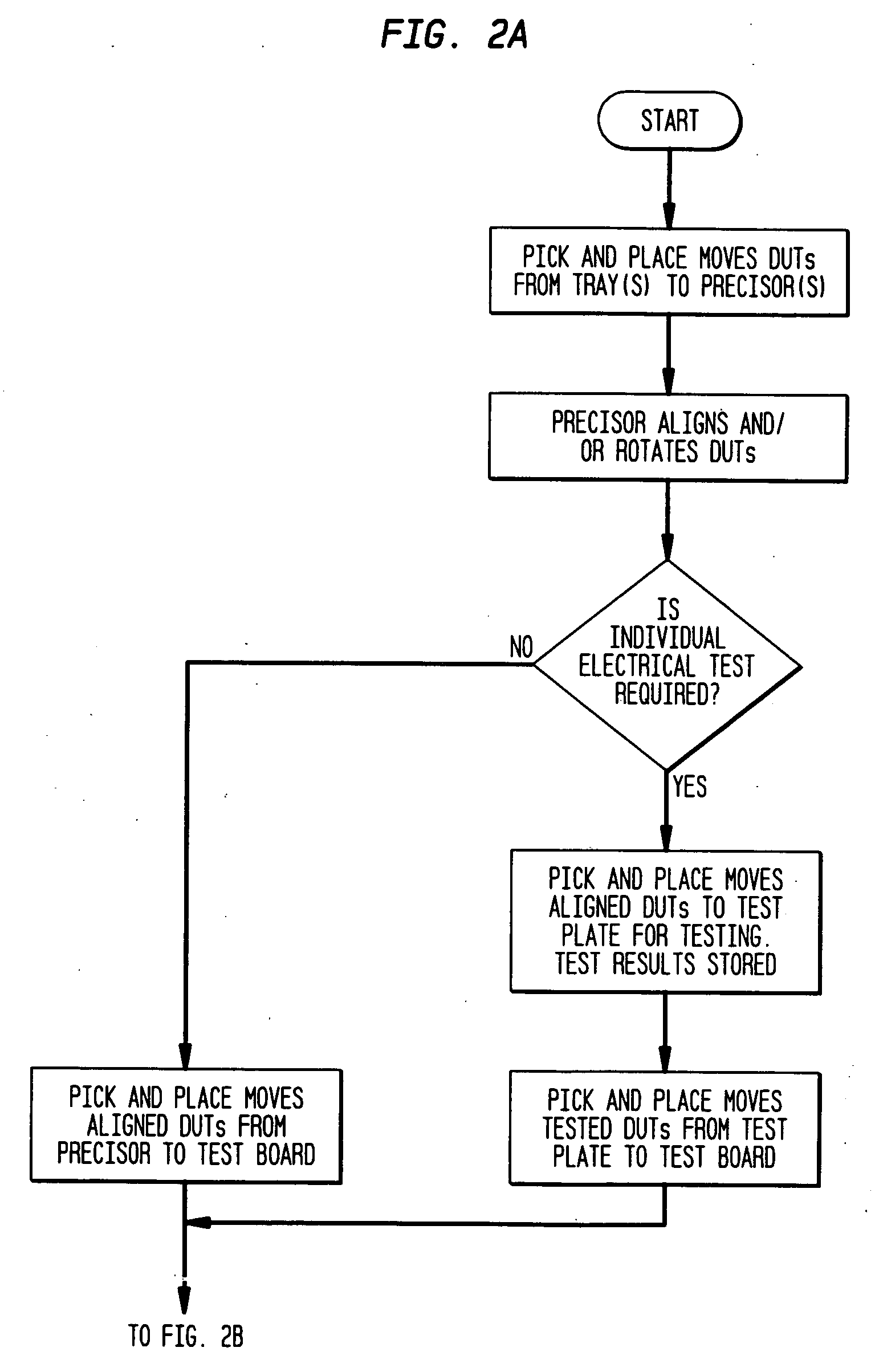
[0041] An embodiment of the process of the present invention is described with reference to the process flow diagrams in FIG. 2A-2C. Referring to FIG. 2A, the process starts by causing the pick-and place apparatus to pick DUTs from the carrier tray in which the DUT is supplied (e.g. JDEC trays) and place the DUT in an alignment stage referred to as a precisor plate. In the precisor plate, the DUT is rotated (if its orientation is not suited to proper placement in a test socket) and aligned. After alignment the pick-and-place apparatus' next step depends upon an instruction on the mode of test. If the test mode is one that requires the DUT to be subjected to an individual electrical test, the pick-and-place apparatus removes the DUT from the precisor and places it into a test plate for the individual electrical test that requires isolated electrical circuitry. After the individual test is performed, the pick-and-place mechanism takes the DUT from the test plate and inserts it into a ...


PUM


Abstract

A method for testing integrated circuit devices and loading such devices into a test board for further testing and an apparatus therefor is disclosed. The method allows for selection between two modes of operation. In a first mode, the integrated circuit devices are subjected to an electrical test before being placed into the test board for further testing. In a second mode, the integrated circuit devices are tested after being placed in the test board. The apparatus allows for the selection between the first mode and the second mode. In either mode, information about the tested devices and the sockets in the test board is used to load the test boards intelligently. Intelligent loading means that devices under test (DUTs) are not placed in bad sockets and devices that do test bad are removed from the test board, with an option of replacing the failed DUT with another DUT before subsequent environmental testing of the DUTs in the test board is carried out.

Description

BACKGROUND OF THE INVENTION [0001] The present invention relates generally to an apparatus and method for testing semiconductor devices. More particularly, the present invention relates to a test apparatus for packaged semiconductor devices that utilizes a pick-and-place mechanism to transfer the devices between and among various locations in the apparatus. [0002] Integrated circuit (IC) devices are subjected to a variety of tests after fabrication. These tests occur before the IC is packaged and after the IC is packaged. The tests are designed to determine if the IC will meet performance and lifetime specifications. [0003] Apparatus with many different configurations are used to test IC devices. In many apparatus, such as the apparatus described in U.S. Pat. No. 6,323,666 to Ohba et al., the IC's are loaded into some sort of test board for environmental testing. Typically, the apparatus performs some initial electrical tests on the IC before subjecting the device to the environment...

Claims


Application Information

Patent Timeline
IPC IPC(8): G01R31/28
CPCG01R1/0408G01R31/2867G01R31/2849G11C2029/5602G11C29/56016G11C29/06G01R31/26H01L22/00
Inventor GOPAL, BALLSONTEONG, CHING PENGLIM, SAMUEL SYN SOO
Owner KES SYST
Why Eureka
Try Eureka