

Semiconductor memory
a technology of semiconductors and memory, applied in the field of semiconductor memory, can solve the problems of high manufacturing cost, inability to control the magnetization direction of mtj elements in the way of fabrication,
- Summary
- Abstract
- Description
- Claims
- Application Information
AI Technical Summary
Problems solved by technology
Method used
Image

Examples
first embodiment
(1) First Embodiment
[1] Overview
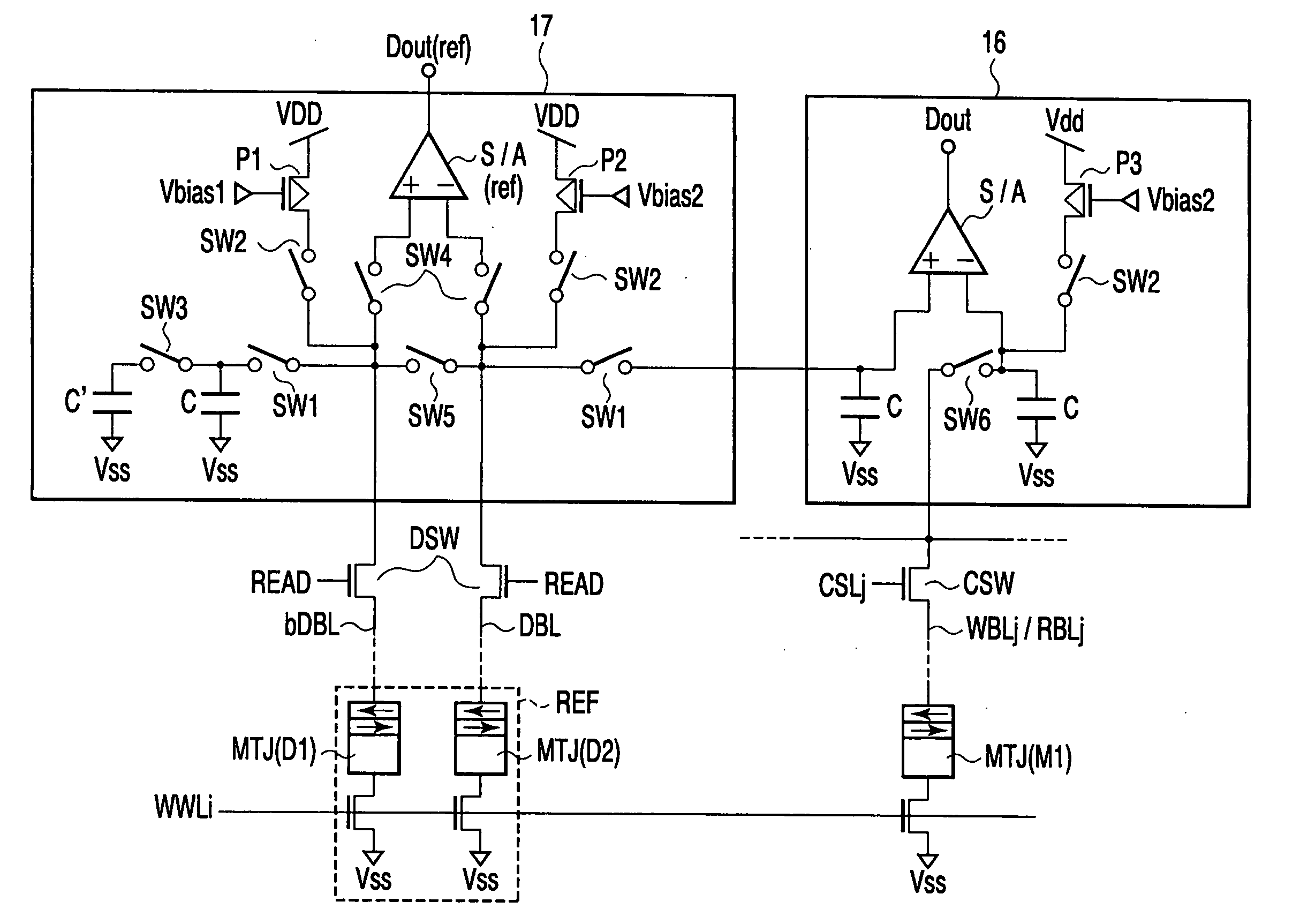
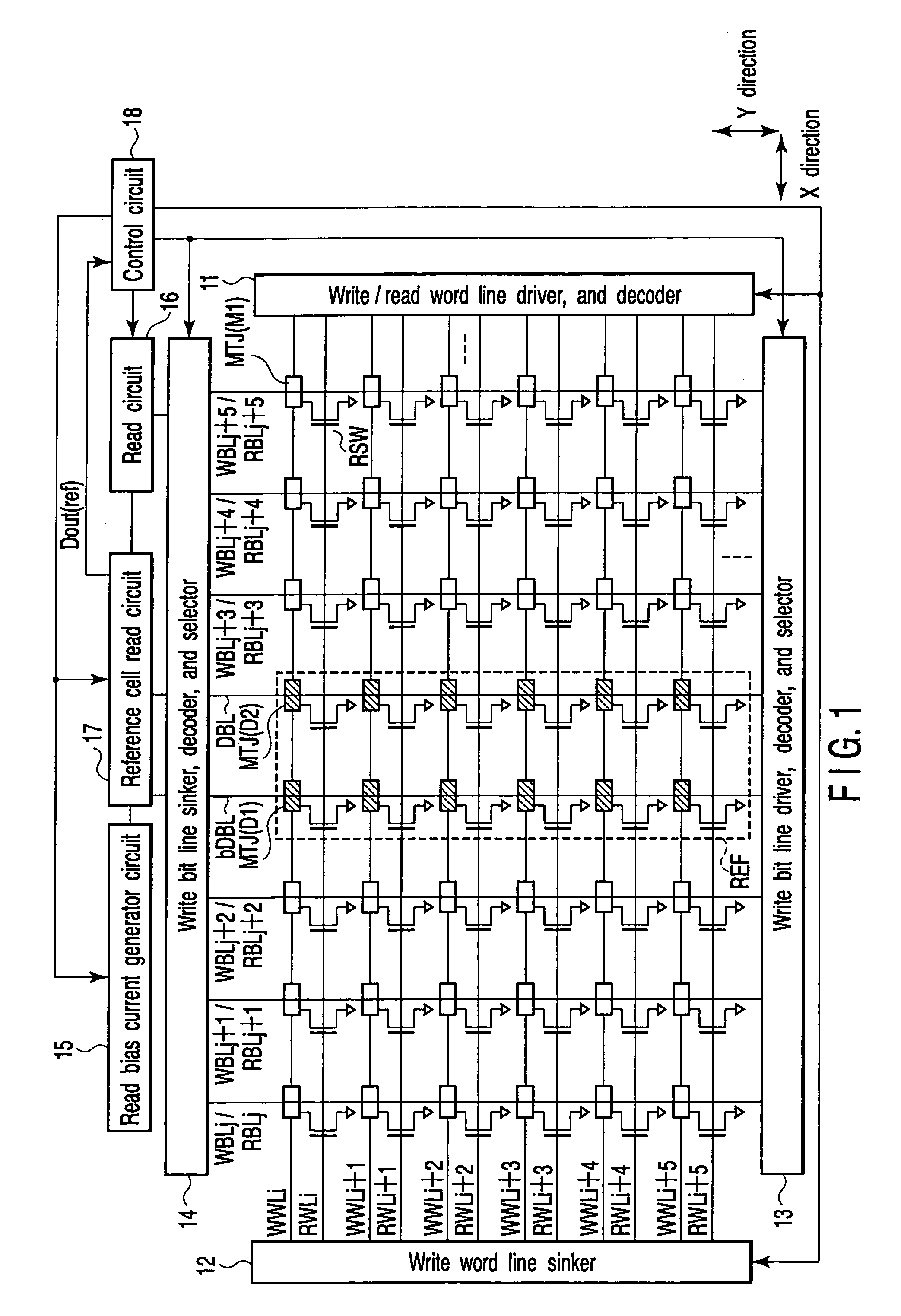
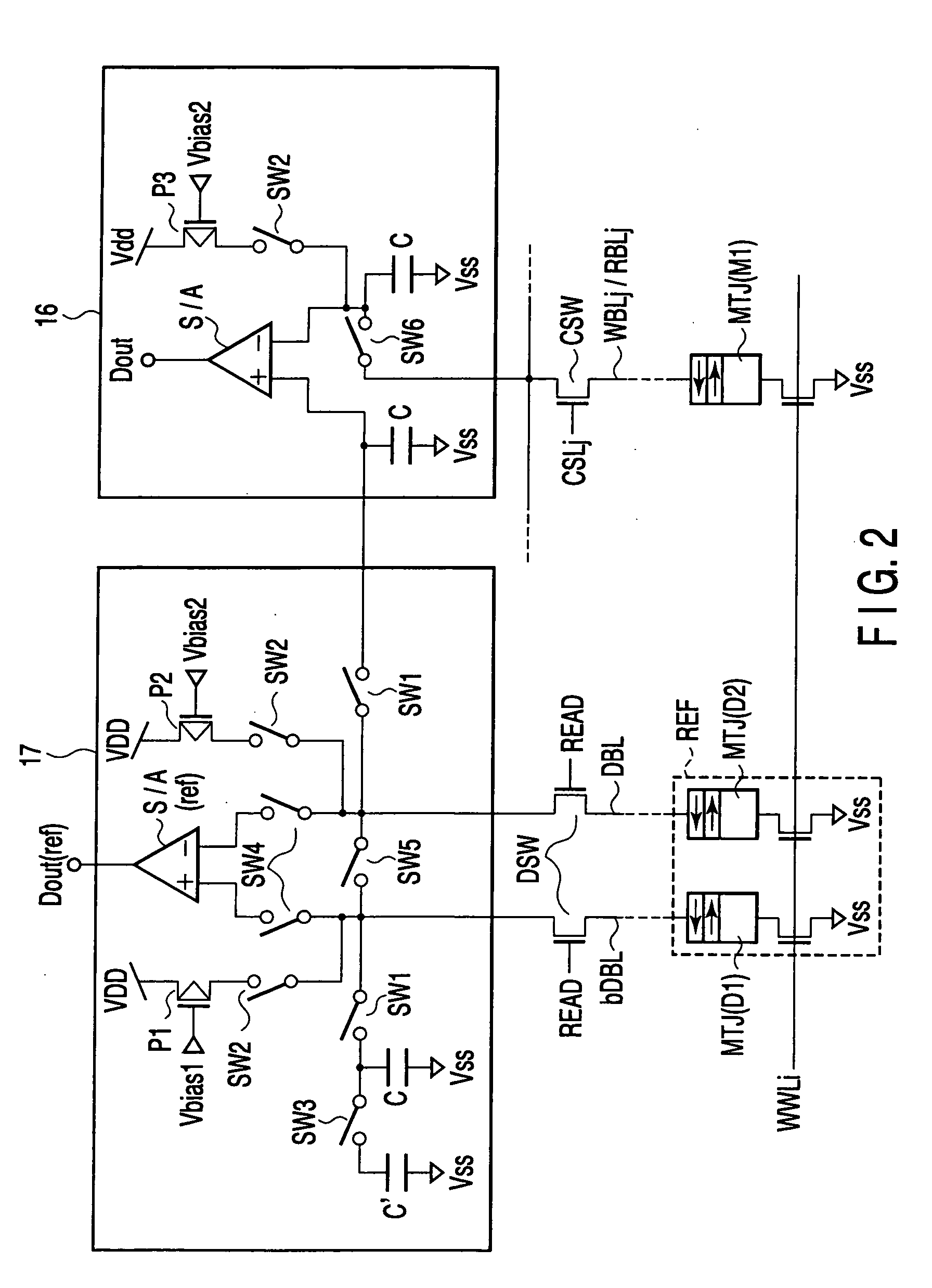
[0039]FIG. 1 shows essential portions of a magnetic random access memory according to a first embodiment of the present invention.
[0040] A memory cell array has a one-transistor, one-MTJ type cell array structure. That is, one memory cell is composed of one read selector switch (transistor) RSW and one MTJ element MTJ.
[0041] On the memory cell array, there are allocated: write word lines WWLi, . . . and read word lines RWLi, . . . which extend in an X direction; and write / read bit lines WBLj / RBLj, . . . and reference bit lines DBL, bDBL which extend in a Y direction.
[0042] An MTJ element MTJ(M1) of a memory cell is allocated at a crossing portion between the write word lines WWLi, . . . and the write / read bit lines WBLj / RBLj, . . . . In addition, MJT elements MTJ(D1) and MTJ(D2) of reference cells are allocated at a crossing portion between the write word lines WWLi, . . . and reference bit lines DBL and bDBL.
[0043] The read word line RWLi, . . ...
second embodiment
(2) Second Embodiment
[0150] The present embodiment relates to a sequence for setting a data value in response to a reference cell relating to an embodiment of the present invention. The present embodiment is featured in that detection of whether or not data in a reference cell is set to its target value is carried out by adjusting a bias current applied to an MTJ element.
[1] Overview
[0151]FIG. 8 shows essential portions of a magnetic random access memory according to a second embodiment of the present invention.
[0152] The overview is identical to that of the magnetic access memory shown in FIG. 1. A detailed description is omitted here.
[0153] In the present embodiment, when a data value is set in response to a reference cell, a read current (bias current) applied to the MTJ element is adjusted by using the reference cell read circuit 17, and it is detected whether or not the MTJ element connected to the reference bit line bDBL is set to “0”, and the MTJ element connected to the...
third embodiment
(3) Third Embodiment
[0217] The present embodiment relates to a sequence for setting a data value in response to a reference cell relating to an embodiment of the present invention. The present embodiment is featured in that detection of whether or not data in a reference cell reaches a target value is carried out by making characteristics of a sense amplifier in a reference cell read circuit different from those of a current sense amplifier.
[1] Overview
[0218]FIG. 11 shows essential portions of a magnetic random access memory according to a third embodiment of the present invention.
[0219] The overview is identical to that of the magnetic random access memory shown in FIG. 1. A detailed description is omitted here.
[0220] In the present embodiment, the characteristics of the sense amplifier in the reference cell read circuit 17 are made different from those of a general sense amplifier. Thus, when a data value of a reference cell is set, it is possible to detect whether the MTJ el...
PUM
 Abstract
Description
Claims
Application Information