Coating device and coating film forming method

a technology of coating device and coating film, which is applied in the direction of coatings, photomechanical equipment, instruments, etc., can solve the problems affecting the yield and quality of products, and achieve the effect of excellent uniform thickness

Inactive Publication Date: 2006-03-30
TOKYO ELECTRON LTD
View PDF2 Cites 18 Cited by
  • Summary
  • Abstract
  • Description
  • Claims
  • Application Information

AI Technical Summary

Benefits of technology

[0007] The present invention has been made in consideration of the situations, and it is an object of the present invention to provi...

Problems solved by technology

Recently, as miniaturization of circuit patterns and high integration are advanced, a resist film to be formed becomes ...

Method used


Image

  • Coating device and coating film forming method
  • Coating device and coating film forming method
  • Coating device and coating film forming method

Examples


Embodiment Construction

and the Example;

[0054]FIG. 9 is a graph representing a change in the thickness of the resist film, formed by using the process cup of the Example, in the radial direction of the wafer, with a exhaust pressure changed; and

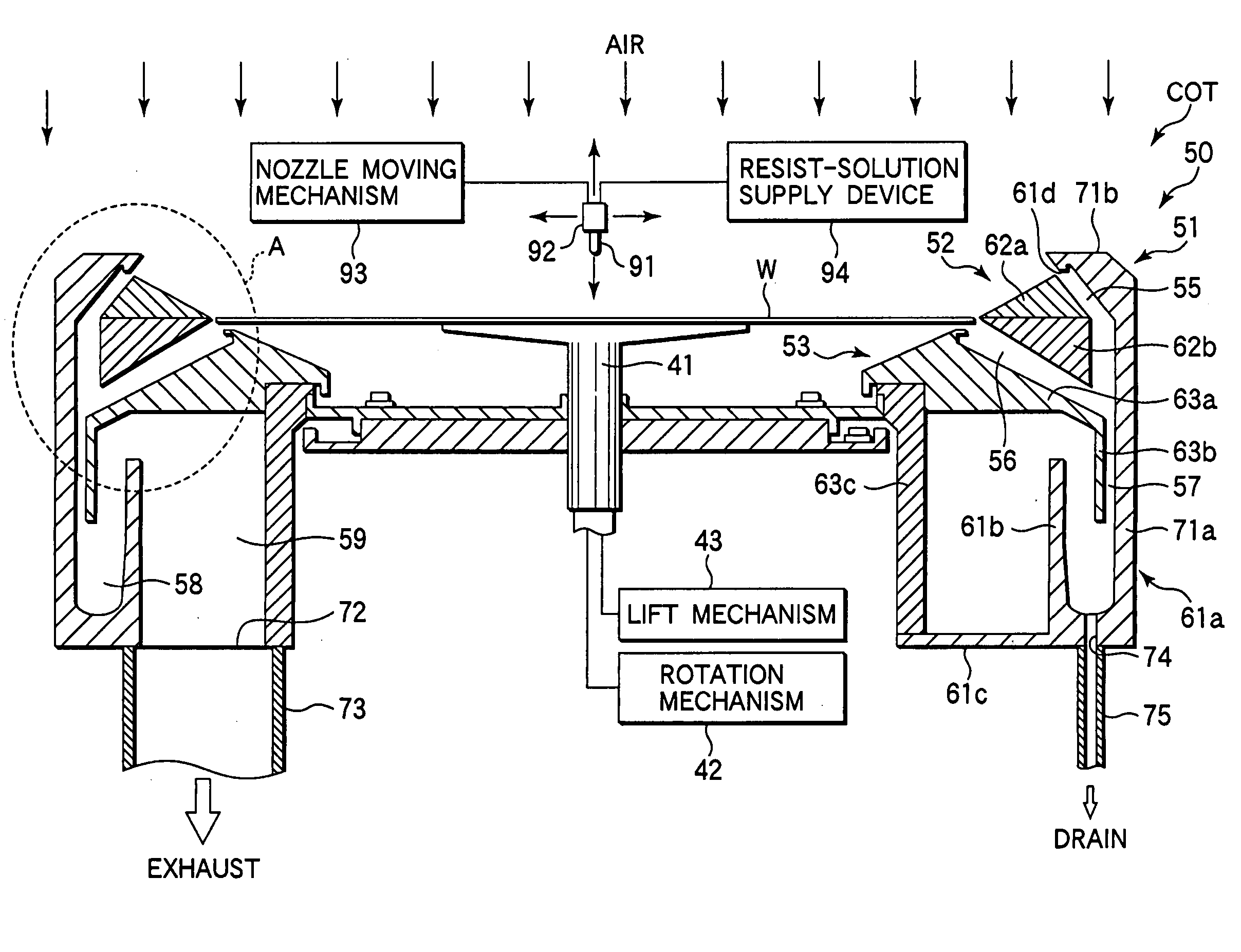
[0055]FIG. 10 is a cross sectional view illustrating the schematic structure of another resist coating unit.

BEST MODE FOR CARRYING OUT THE PRESENT INVENTION

[0056] An embodiment of the present invention will now be described in detail with reference to the accompanied drawings. In this embodiment, one taken as an example is a resist coating and developing apparatus that includes a resist coating unit which forms a resist film by applying a resist liquid to a semiconductor wafer, and caries out a series of processes from the formation of a resist film to the development thereof.

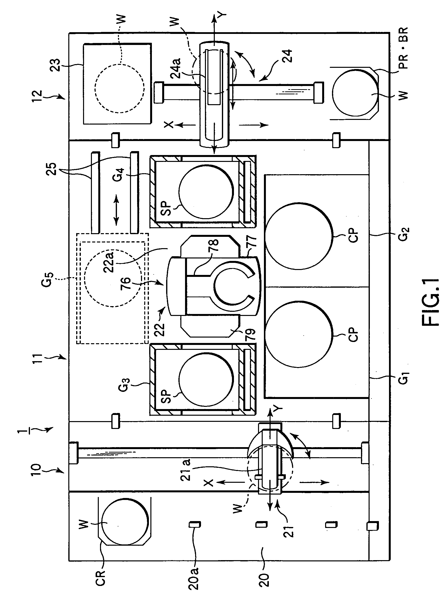
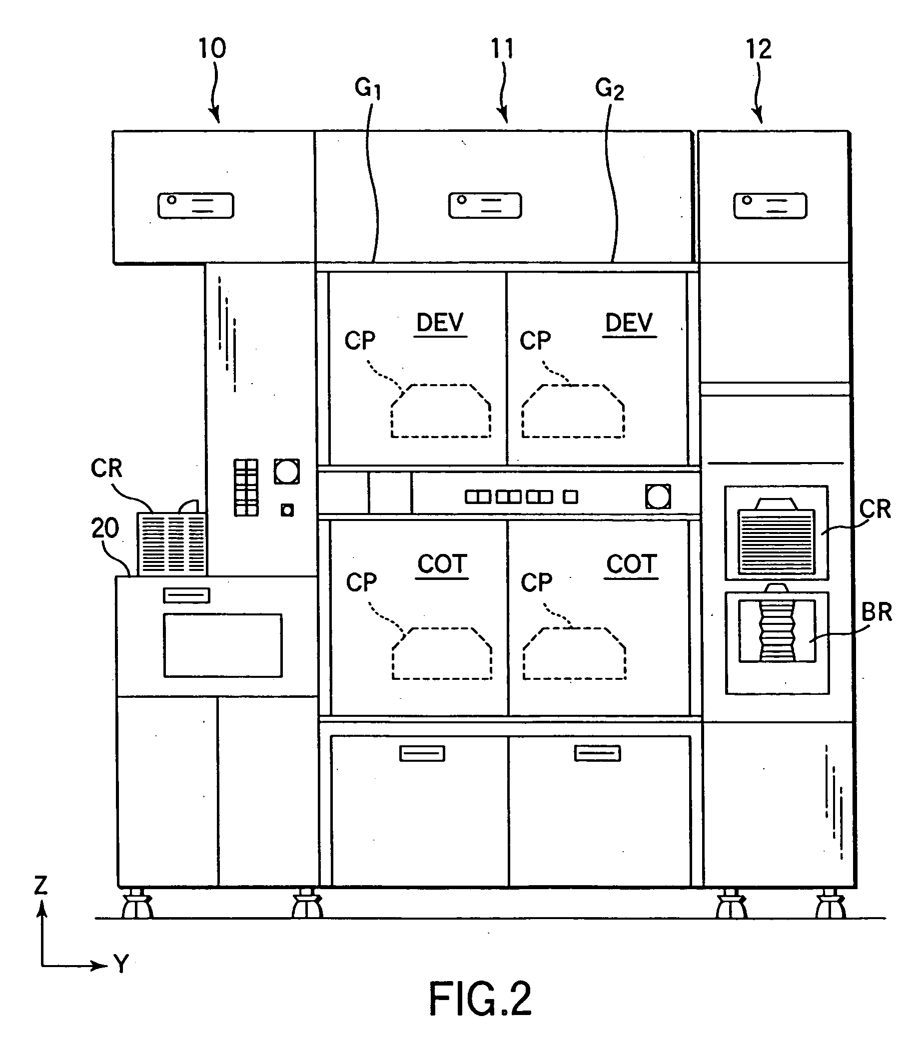
[0057]FIG. 1 is a schematic plan view illustrating a resist coating and developing system 1, FIG. 2 is a front view thereof, and FIG. 3 is a back view thereof. The resist coating and develop...


PUM


Abstract

The resist coating unit (COT) has a spin chuck (41) which holds the wafer to be supplied with a resist liquid, and a process cup (50) which accommodates the spin chuck (41) and exhaustes an atmosphere around the wafer W from a bottom thereof. The process cup (50) comprises a first cup (51) with an outer circumferential wall (61a), and an airflow control member (52) laid out close to the wafer W in the first cup (51) in such a manner as to surround the wafer W. The airflow control member (52) has a vertical cross section of an approximately rectangular shape defined by the upper ring portion (62a) having a cross section of an approximately triangular shape and protruding upward, and a lower ring portion (62b) having a cross section of an approximately triangular shape and protruding downward. An exhaust passage (55) for substantially exhausting the atmosphere around the wafer W is formed between the outer circumferential wall (61a) and the airflow control member (52).

Description

TECHNICAL FIELD [0001] The present invention relates to a coating process apparatus and a coating film forming method for forming a film by applying a coating liquid to a substrate to be processed. BACKGROUND ART [0002] For instance, in a process of fabricating a semiconductor device, a predetermined circuit pattern is formed on a semiconductor wafer by using the photolithography technology. According to this photolithography process, a resist film is formed on a wafer, the resist film is exposed in a predetermined pattern, and then the exposed wafer is developed, whereby the circuit pattern is formed thereon. [0003] As a method of forming a resist film on a wafer, so-called spin coating is widely used, which supplies a predetermined amount of a resist liquid is supplied to the center portion of a wafer held substantially horizontally and then rotates the wafer at a high speed so as to spread the resist liquid over the entire wafer surface. [0004] Unexamined Japanese Patent Applicat...

Claims


Application Information

Patent Timeline
IPC IPC(8): B05C13/00B05C11/02B05D3/12B05C11/08G03F7/16H01L21/00H01L21/027
CPCG03F7/162H01L21/6715H01L21/67017
Inventor SHITE, HIDEO
Owner TOKYO ELECTRON LTD
Why Eureka
Try Eureka