Method and device for plasma cvd

a plasma and cvd technology, applied in the field of plasma cvd methods and devices, can solve the problems of enlargement of the whole manufacturing apparatus, increased cost, and difficult to obtain thin films of excellent uniform thickness, and achieve the effect of high productivity

Inactive Publication Date: 2004-03-18
IHI CORP
View PDF12 Cites 11 Cited by
  • Summary
  • Abstract
  • Description
  • Claims
  • Application Information

AI Technical Summary

Benefits of technology

0011] It is also possible to realize the plasma CVD apparatus with a high productivity by arranging at least three electrode array layers, each of which has a plurality of inductively coupled electrodes forming one plane, and arranging the substrate holder between two electrode array layers.

Problems solved by technology

Consequently, the film thickness in the central part of substrate is different from that in the circumference part, meaning that the thin film of excellent uniform thickness is hard to be obtained.
Thus, if higher throughput is requested, two sets of apparatuses shown in FIG. 8(b) must be installed, which invites the enlargement of the whole manufacturing apparatus and its cost increase.

Method used


Image

  • Method and device for plasma cvd
  • Method and device for plasma cvd
  • Method and device for plasma cvd

Examples


first embodiment

[0024] (First Embodiment)

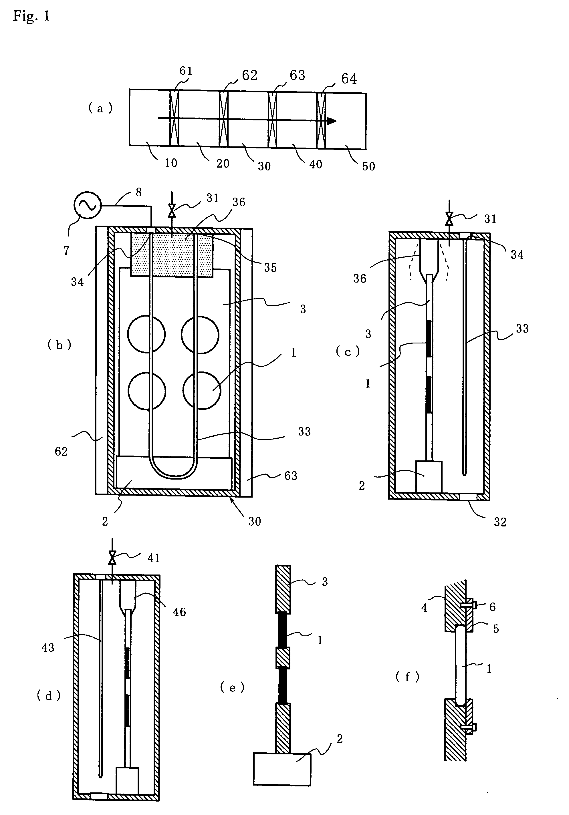
[0025] The first embodiment of this invention is shown in FIG. 1. FIG. 1 is a schematic view showing an example of the plasma CVD apparatus used for manufacturing solar cells shown in FIG. 7.

[0026] As is shown in FIG. 1(a), a plasma CVD apparatus is composed of a load lock chamber 10, a heating chamber 20, a first plasma CVD (PCVD) chamber 30, a second PCVD chamber 40, and a cooling chamber 50. These chambers are connected through gate valves 61-64. The substrates 1 are held by a substrate holder 3 so that both thin film formation surfaces of substrate are exposed, for example, by pressing the circumference portion of substrate with a plate 4 having apertures and press plates 5, and fixing them with screws 6, as shown in FIG. 1(f)

[0027] The substrate holder 3 holding a plurality of substrates is fixed on a carrier 2 (FIG. 1(e)), and transported along the rails constructed in the chambers in the direction of arrow shown in FIG. 1(a) to process the substrates ...

second embodiment

[0036] (Second Embodiment)

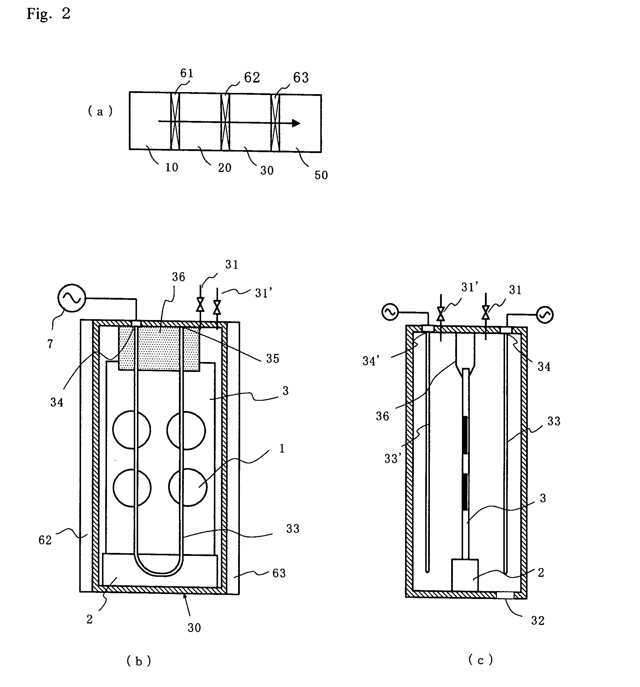
[0037] Although the p-type and n-type a-Si films are formed in the different PCVD chambers in the plasma CVD apparatus of FIG. 1, it is also possible to form different films on respective surfaces of substrate in one PCVD chamber. The embodiment for this purpose is shown in FIG. 2. As shown in FIG. 2(a), the whole apparatus is nearly the same as that shown in FIG, 1, except that the number of PCVD chamber is one.

[0038] As shown in FIGS. 2(b) and 2(c), two inductively coupled electrodes, whose power feeding portions 34, 34' are connected to high-frequency power sources, are arranged in plasma CVD chamber 30. The substrate holder is transported into the PCVD chamber and placed between these two electrodes. In addition, two gas supply pipe lines 31, 31' for two film forming gases (SiH.sub.4 / PH.sub.3 gas and SiH.sub.4 / B.sub.2H.sub.6 gas) are connected to the PCVD chamber.

[0039] When the substrate holder is transported into PCVD chamber 30, SiH.sub.4 / PH.sub.3 ga...

third embodiment

[0042] (Third Embodiment)

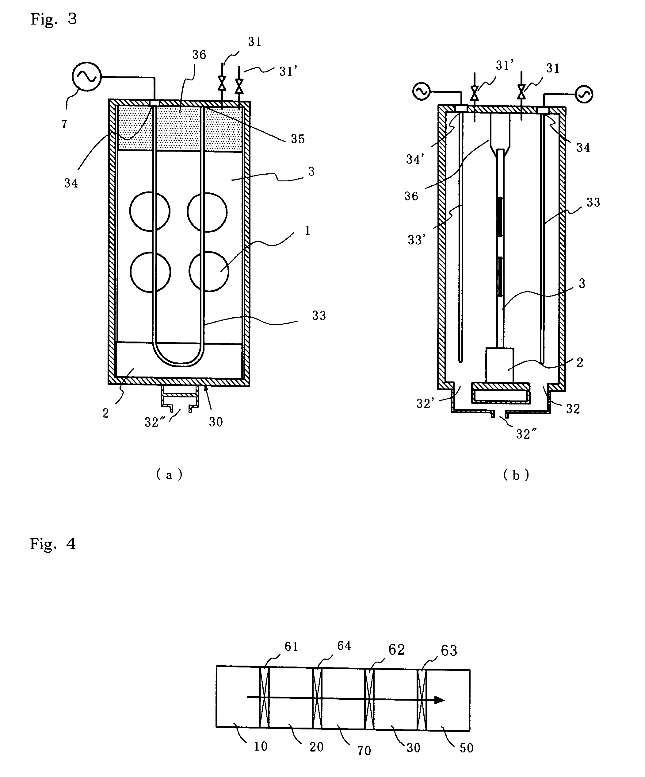
[0043] In the example of FIG. 2, the p-type a-Si film is formed after the n-type a-Si film is formed. It is also possible in this invention to simultaneously form two different films. The third embodiment which makes possible simultaneous formation of different films is shown in FIG. 3.

[0044] The apparatus has nearly the same configuration as that of FIG. 2(a), except for the PCVD chamber. The PCVD chamber of this embodiment, which is shown in FIG. 3, differs from that shown in FIGS. 2(b) and 2(c) in the following points. That is, in the case of FIG. 2, the blockage is provided to prevent plasma generated in one film forming space for the n-type a-Si film or p-type a-Si film from diffusing to the other film forming space and depositing on the p-type a-Si film or n-type a-Si film, respectively. However, in the third embodiment, the length of substrate holder fixing jig 36 should be made as close as possible to the length of chamber, so that it can act as the ...


PUM

PropertyMeasurementUnit
distanceaaaaaaaaaa
circumferenceaaaaaaaaaa
frequencyaaaaaaaaaa

Abstract

The objective of the present invention is to provide a plasma CVD method and plasma CVD apparatus, which makes it possible to form thin films of excellent uniform thickness on both surfaces of a substrate without the step of turning a substrate over. The present invention is characterized in that at least two inductively coupled electrodes with a power feeding portion and a grounded portion are arranged in a vacuum chamber equipped with a gas supply port and an exhaust port, a substrate holder which holds a substrate at a circumference portion so that both surfaces of the substrate are exposed is transported into between said two inductively coupled electrodes, and a film forming gas is introduced through the gas supply port, and high-frequency power is fed to the power feeding portion to generate plasma along the inductively coupled electrode to form a thin film on both surfaces of the substrate simultaneously or one by one. Furthermore, a second gas supply system is connected to the vacuum chamber to form different film on respective surfaces of the substrate simultaneously or one by one.

Description

[0001] The present invention relates to a Plasma CVD method and a Plasma CVD apparatus and, more particularly, to the Plasma CVD method and apparatus for forming thin films of excellent uniform thickness on both surfaces of a substrate.BACKGROUND OF INVENTION[0002] A solar cell generally consists of a p-n junction or p-i-n junction with silicon (Si) or compound semiconductors formed on a substrate to convert sunlight incident onto its front surface into electricity. In order to increase the electric power generation, a solar cell utilizing sunlight incident on the back surface as well as front surface is proposed. Such a solar cell has, for example, a configuration shown in FIG. 7, and is fabricated by depositing a p-type amorphous Si (p-type a-Si) film 102 and an n-type amorphous Si (n-type a-Si) film 103 on the respective surfaces of i-type crystal silicon 101 using a plasma CVD method, and then by forming a transparent electrode 104 using a sputtering method and current collectiv...

Claims


Application Information

Patent Timeline
Patent Type & Authority Applications(United States)
IPC IPC(8): B01J19/08C23C16/509H01J37/32H05H1/46H01L21/205H01L31/04
CPCH01J37/321C23C16/509H01L21/205
Inventor ITO, NORIKAZU
Owner IHI CORP
Why Eureka
Try Eureka