Process for manufacture of novel, inexpensive radio frequency identification devices

a radio frequency identification and inexpensive technology, applied in the direction of mechanical actuation of burglar alarms, near-field systems using receivers, instruments, etc., can solve the problems of insufficient chip alignment, high cost, time-consuming and environmental hazards, and current manufacturing using photolithographic methods

Inactive Publication Date: 2006-04-06
ELECTROX
View PDF17 Cites 217 Cited by
  • Summary
  • Abstract
  • Description
  • Claims
  • Application Information

AI Technical Summary

Problems solved by technology

Current manufacturing utilizes photolithographic methods which are costly, time consuming and can be environmentally hazardous.
While researchers are describing ways to “print” organic transistors or nano-particle inorganic transistors for RFID; their perf

Method used


Image

  • Process for manufacture of novel, inexpensive radio frequency identification devices
  • Process for manufacture of novel, inexpensive radio frequency identification devices
  • Process for manufacture of novel, inexpensive radio frequency identification devices

Examples


examples

[0035] The examples described below indicate how the individual constituents of the preferred compositions and the conditions for applying them function to provide the desired result. The examples will serve to further typify the nature of this invention, but should not be construed as a limitation in the scope thereof which scope is defined solely in the appended claims.

example i

[0036] A 25 micron thick PET film was coated with Saran® resin #F-276 (DOW) to a nominal thickness of 1 micron. Parmod Silver Toner E-43 (Parelec LLC, Rocky Hill, N.J.) was mixed to 1.5% by weight concentration to a conductivity of 5 pico siemens per cm. This toner was then imaged on a standard Electrox electrostatic printing plate (Dynachem #5038 dry film etch resist, exposed to a level of 250 mj / cm2). The silver toner image was transferred to the Saran coated PET film. The toner mage was dried at about 40° C.

[0037] Next a silicon chip thinned to 10 microns by means practiced by Virginia Semiconductor Inc. of Richmond, Va. was placed, active side down onto the silver toner image. The assembly of silicon chip on toner image on coated PET film was heated to 125° C. for two minutes. Good conductivity of the silver was achieved with excellent bonding of the chip to the silver.

example ii

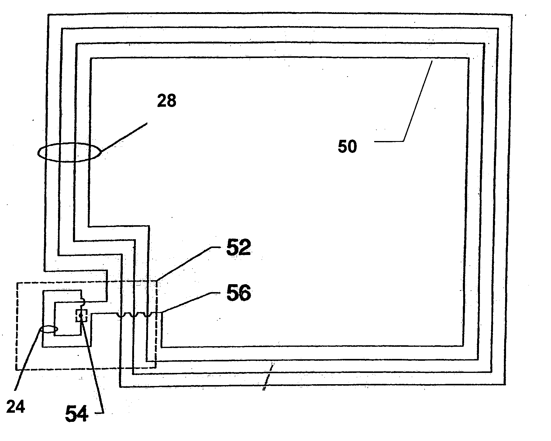
[0038] A three layer substrate was prepared using the same techniques of Example 1. A Saran coated PET film was imaged with Parmod toner and thermally cured into a useful conductive pattern. A dielectric “cross over” pattern of a Saran toner was printed and reflowed into a pin hole free layer. Note, the electrode pads of the conductive pattern of the first layer are left uncovered by the Saran cross-over layer. A second metal layer was printed on the Saran layer interconnecting the electrodes.

[0039] A portion of the pattern of the first layer and the pattern of the second metal layer were configured to form a coil pattern (“secondary winding”).

[0040] A dot of thermally or pressure activated adhesive was applied to the “secondary winding” region of the substrate and a silicon die with a “primary winding” contained on its surface was accurately placed on this adhesive. Bonding is completed by heat or pressure.


PUM

PropertyMeasurementUnit
Lengthaaaaaaaaaa
Thicknessaaaaaaaaaa
Thicknessaaaaaaaaaa

Abstract

A novel process for fabricating low cost RFID devices in which a pattern of metallic toner is printed on a substrate and the contacts on a silicon die are placed directly on contact points printed as part of the pattern of metallic toner; the whole device is then heated to both cure the metallic toner into metallic conductors and bond the silicon die to the metallic conductors. Alternatively, the silicon die can be physically attached to the substrate and the electrical pathway between the silicon die and the metallic conductors is established via a transformer coupling comprised of a coil winding on the silicon die and a pattern of coils printed as part of the metallic toner pattern. The pattern of coils can be comprised of individually printed coil loops printed on, and separated by, dielectric layers.

Description

CROSS REFERENCE TO RELATED APPLICATIONS [0001] This application claims the priority of U.S. Provisional Patent Application Ser. No. 60 / 255,490 filed Dec. 15, 2000, the entire contents and subject matter of which is hereby incorporated in total by reference.BACKGROUND OF THE INVENTION [0002] 1. Field of the Invention [0003] This invention describes methods for the manufacture of inexpensive radio frequency identification devices (RFID) that are also very thin in cross section so that they can be laminated into paper, tags or labels without mechanical interference nor surface distortion. [0004] 2. Description of the Related Art [0005] Radio frequency identification and tracking devices (RFID) have shown a rapid growth in both function and capabilities. RFIDs are currently used in everything from anti theft tags, to smart wireless cards to identification tags for merchandise and many other uses are in the design / system specification stage. Examples of currently available systems which ...

Claims


Application Information

Patent Timeline
IPC IPC(8): G06K19/06G08B13/14H01Q17/00G06K19/07G06K19/077H01L21/60H01L23/31H01L23/498H01Q1/22H01Q1/44H01Q7/00H04B5/02
CPCG06K19/07749Y10T29/49018G06K19/07756G06K19/07775G06K19/07779G06K19/07783G06K19/07784G08B13/2417G08B13/2437H01L23/3121H01L23/49855H01L24/81H01L24/83H01L2224/81801H01L2224/8319H01L2224/838H01L2924/01005H01L2924/01013H01L2924/01027H01L2924/01029H01L2924/01039H01L2924/01047H01L2924/01075H01L2924/01079H01L2924/0781H01L2924/19042H01Q1/22H01Q1/2225H01Q1/44H01Q7/00H01Q9/27H01L24/29H01L2224/2919H01L2224/29298H01L2924/01006H01L2924/0665G06K19/0775H01L2924/00013H01L2924/10253H01L2924/00014H01L2924/00H01L2224/29099H01L2224/29199H01L2224/29299H01L2224/2929
Inventor DETIG, ROBERTHBREMBERG, VERNONL
Owner ELECTROX
Why Eureka
Try Eureka