Method and apparatus for controlling temperature of a substrate

a technology of substrate temperature and temperature control, applied in the direction of mechanical apparatus, chucks, manufacturing tools, etc., can solve the problems of insufficient means for controlling the temperature distribution of substrate temperature across the diameter of the substrate, the inability to control the temperature uniformity of the substrate, and the adverse effect of process uniformity

Inactive Publication Date: 2006-04-13
APPLIED MATERIALS INC
View PDF24 Cites 192 Cited by
  • Summary
  • Abstract
  • Description
  • Claims
  • Application Information

AI Technical Summary

Benefits of technology

[0007] The present invention generally is a method and apparatus for controlling temperature of a substrate during processing the substrate in a semiconductor substrate processing apparatus. The method and apparatus enhances temperature control across the diameter of a substrate, and may be utilized in etch, deposition, implant, and thermal processing systems, among other applications where the control of the temperature profile of a workpiece is desirable.
[0008] In one embodiment of the invention, a substrate pedestal assembly is provided. The pedestal assembly includes a support member that is coupled to a base using a material layer. The material layer has at least two regions having different coefficients of thermal conductivity. In another embodiment, the support member is an electrostatic chuck. In further embodiments, a pedestal assembly has channels formed between the base and support member for providing cooling gas in proximity to the material layer to further control heat transfer between the support member and the base, thereby facilitating control of the temperature profile of a substrate disposed on the support member.

Problems solved by technology

During processing, changes in the temperature and temperature gradients across the substrate may be detrimental to material deposition, etch rate, step coverage, feature taper angles, and other parameters of semiconductor devices.
However, conventional substrate pedestals have insufficient means for controlling substrate temperature distribution across the diameter of the substrate.
The inability to control substrate temperature uniformity has an adverse effect on process uniformity both within a single substrate and between substrates, device yield and overall quality of processed substrates.

Method used


Image

  • Method and apparatus for controlling temperature of a substrate
  • Method and apparatus for controlling temperature of a substrate
  • Method and apparatus for controlling temperature of a substrate

Examples


Embodiment Construction

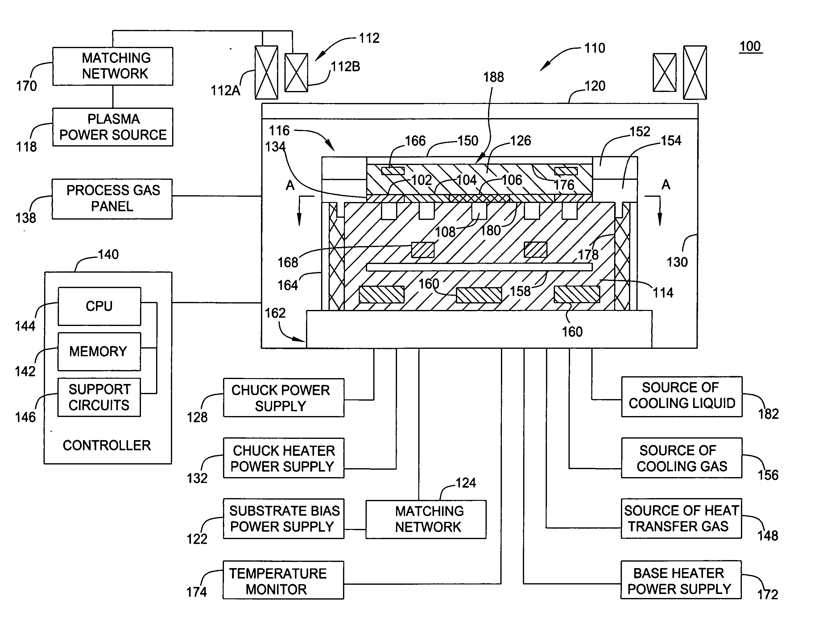
[0018] The present invention generally is a method and apparatus for controlling temperature of a substrate during processing. Although invention is illustratively described in a semiconductor substrate processing apparatus, such as, e.g., a processing reactor (or module) of a CENTURA® integrated semiconductor wafer processing system, available from Applied Materials, Inc. of Santa Clara, Calif., the invention may be utilized in other processing systems, including etch, deposition, implant and thermal processing, or in other application where control of the temperature profile of a substrate or other workpiece is desirable.

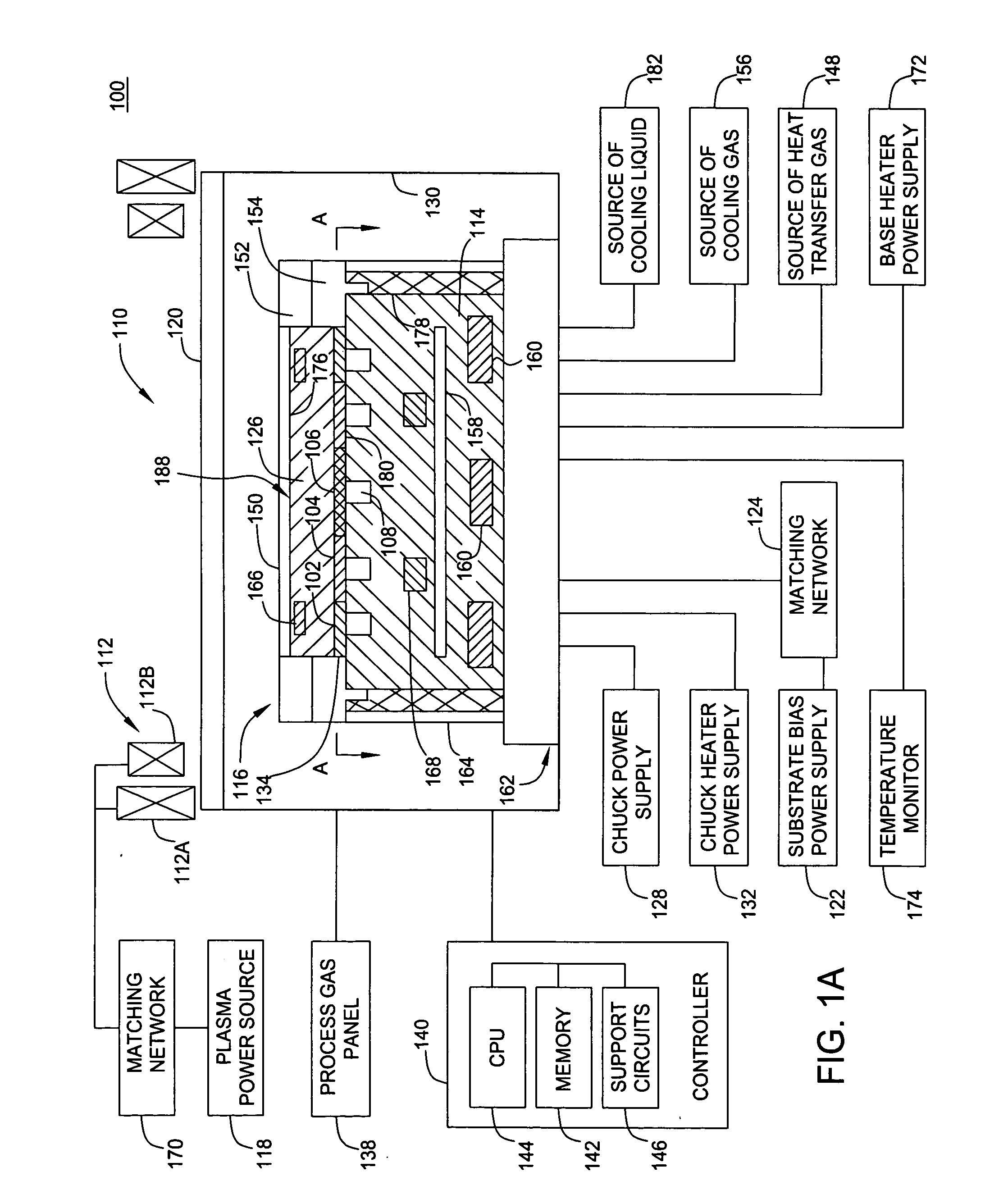
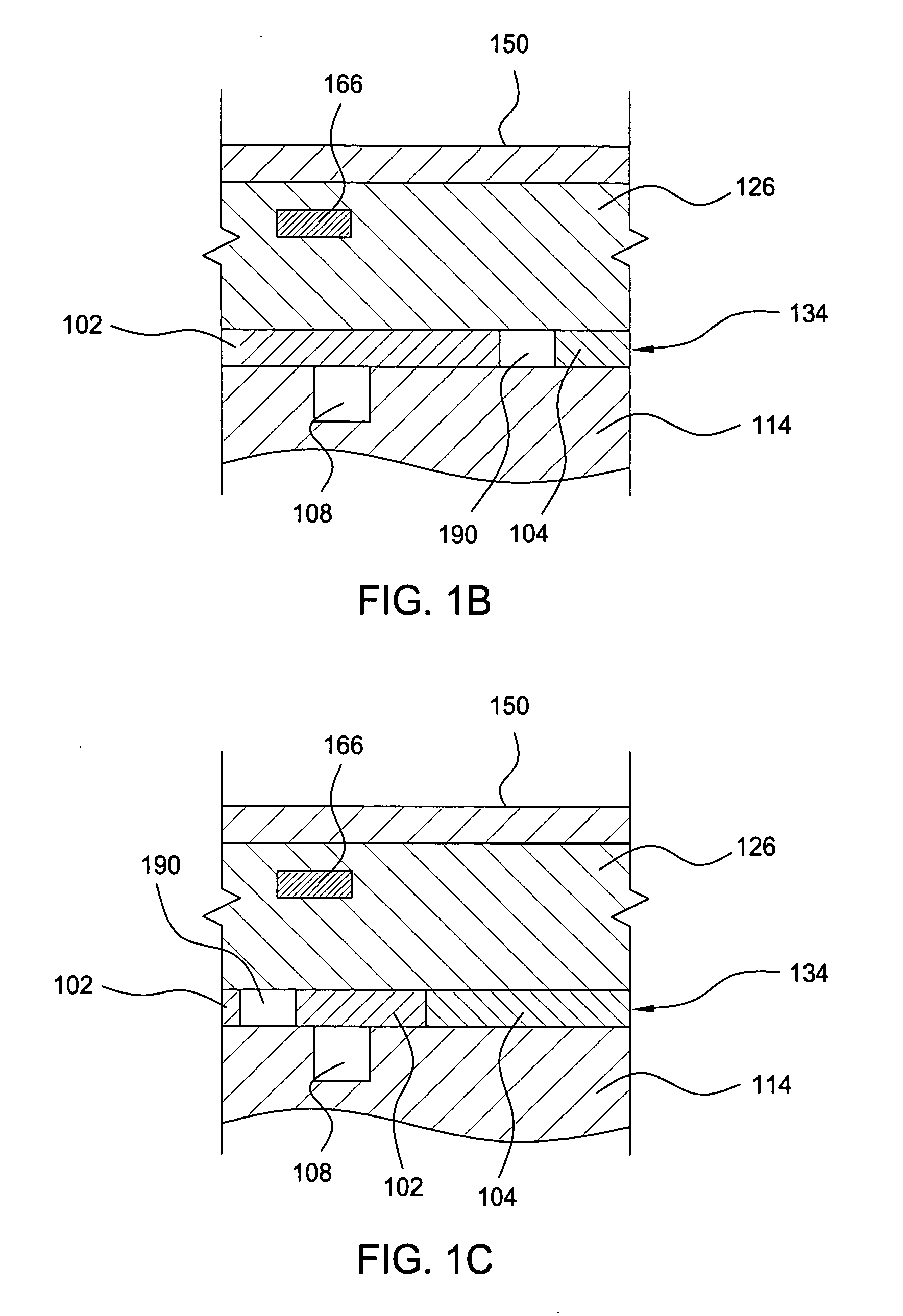
[0019]FIG. 1 depicts a schematic diagram of an exemplary etch reactor 100 having one embodiment of a substrate pedestal assembly 116 that may illustratively be used to practice the invention. The particular embodiment of the etch reactor 100 shown herein is provided for illustrative purposes and should not be used to limit the scope of the invention.

[0020] Etch ...


PUM

PropertyMeasurementUnit
pressureaaaaaaaaaa
atmospheric pressureaaaaaaaaaa
coefficients of thermal conductivityaaaaaaaaaa

Abstract

A pedestal assembly and method for controlling temperature of a substrate during processing is provided. In one embodiment, the pedestal assembly includes a support member that is coupled to a base by a material layer. The material layer has at least two regions having different coefficients of thermal conductivity. In another embodiment, the support member is an electrostatic chuck. In further embodiments, a pedestal assembly has channels formed between the base and support member for providing cooling gas in proximity to the material layer to further control heat transfer between the support member and the base, thereby controlling the temperature profile of a substrate disposed on the support member.

Description

BACKGROUND OF THE INVENTION [0001] 1. Field of the Invention [0002] Embodiments of the present invention generally relate to semiconductor substrate processing systems. More specifically, the invention relates to a method and apparatus for controlling temperature of a substrate in a semiconductor substrate processing system. [0003] 2. Description of the Related Art [0004] In manufacture of integrated circuits, precise control of various process parameters is required for achieving consistent results within a substrate, as well as the results that are reproducible from substrate to substrate. During processing, changes in the temperature and temperature gradients across the substrate may be detrimental to material deposition, etch rate, step coverage, feature taper angles, and other parameters of semiconductor devices. As such, generation of the pre-determined pattern of temperature distribution across the substrate is one of critical requirements for achieving high yield.[0005] In s...

Claims


Application Information

Patent Timeline
Patent Type & Authority Applications(United States)
IPC IPC(8): C03C15/00C23F1/00C23C16/00H01L21/306
CPCH01L21/67103Y10T279/23H01L21/6831H01L21/67248H01L21/02
Inventor HOLLAND, JOHNPANAGOPOULOS, THEODOROS
Owner APPLIED MATERIALS INC
Why Eureka
Try Eureka