Display device

a display device and manufacturing method technology, applied in the direction of solid-state devices, electric lighting sources, electric light sources, etc., can solve the problems of precision and deformation, and achieve the effects of preventing damage and deformation of display devices, high reliability, and simplified steps

Inactive Publication Date: 2006-04-20
SEMICON ENERGY LAB CO LTD
View PDF77 Cites 125 Cited by
  • Summary
  • Abstract
  • Description
  • Claims
  • Application Information

AI Technical Summary

Benefits of technology

[0020] According to the aforementioned structures, the spacer and the insulator may be separated as shown in FIGS. 15 and 18B or continuously connected as shown in FIGS. 24A to 25D. The spacer functions after forming an electroluminescent layer and sealing with a sealing substrate to complete a display device to prevent a damage and deformation of a display device due to a pressure and

Problems solved by technology

However, there is a problem in that a defect occurs due to a precision and a deflection of a mas

Method used


Image

  • Display device
  • Display device
  • Display device

Examples


embodiment mode 1

[0051] A manufacturing method of a display device of this embodiment mode is described with reference to FIGS. 1 to 4.

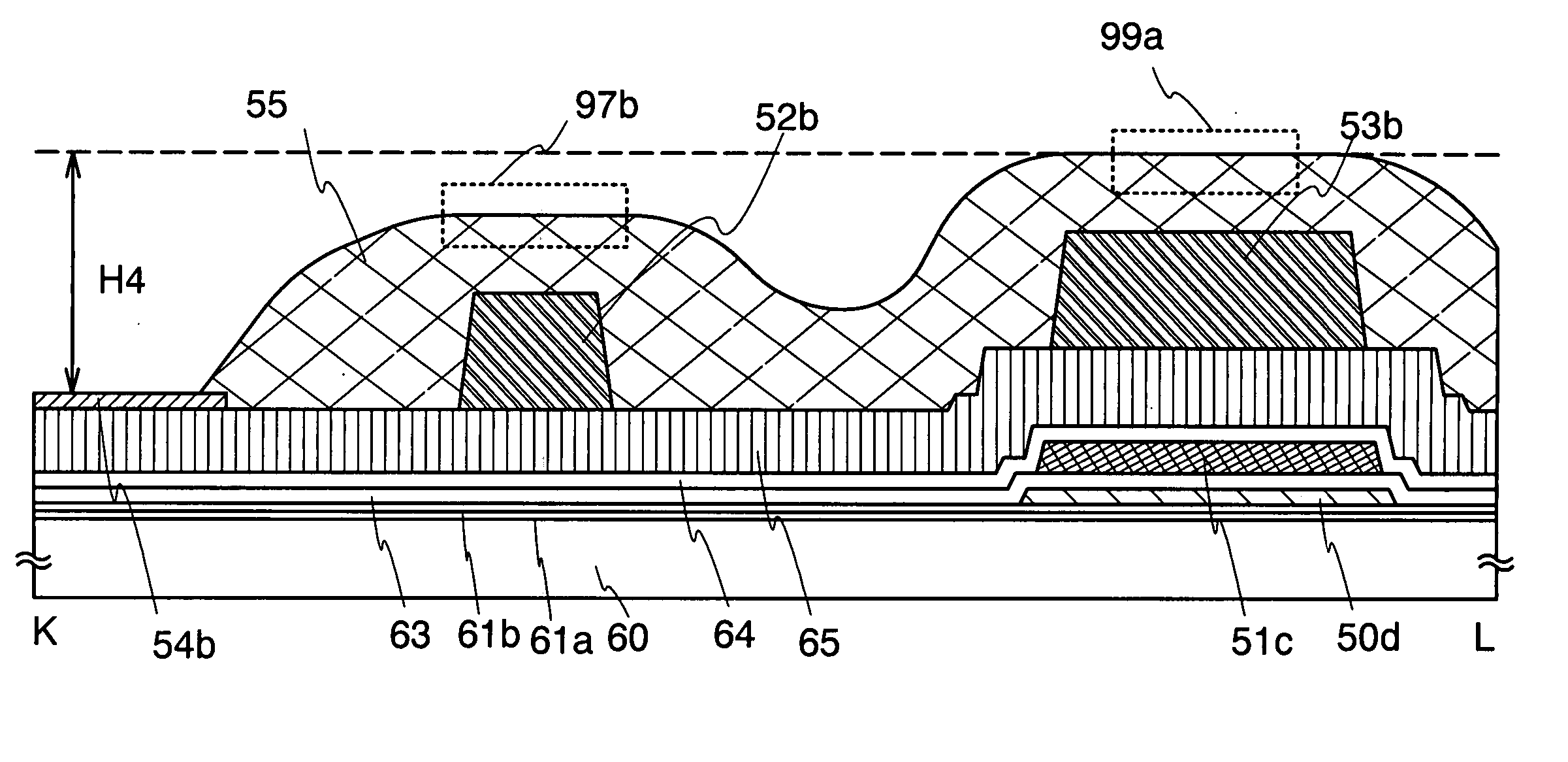
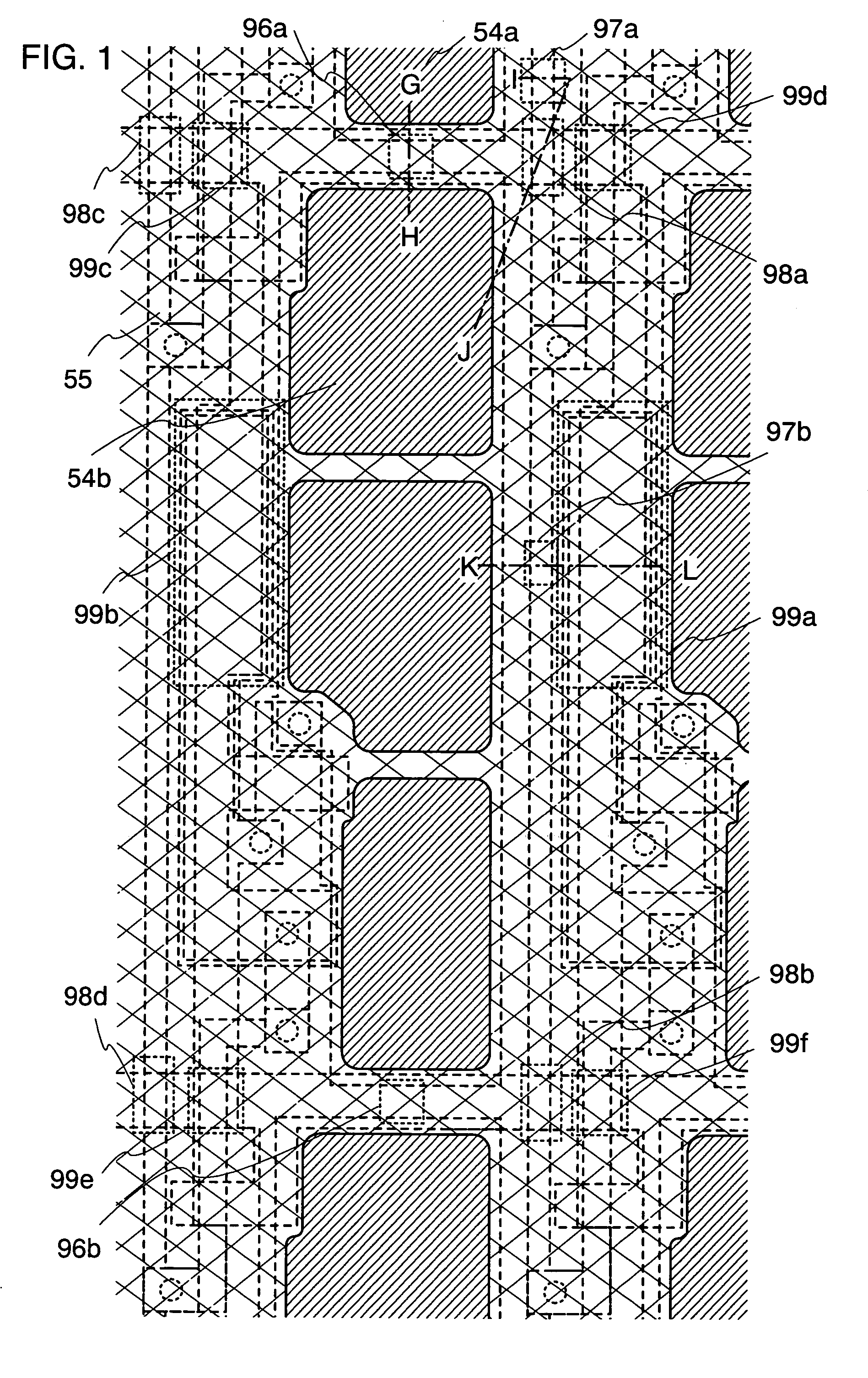
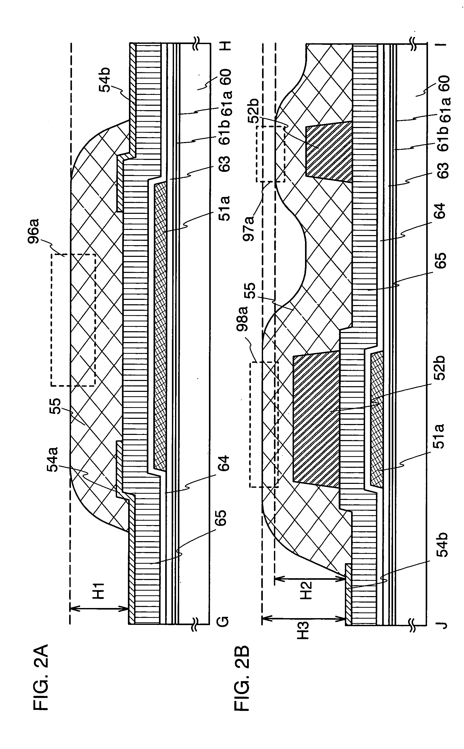
[0052]FIGS. 1 and 4 are top plan views of a pixel region of a display device manufactured using the invention. FIGS. 2A to 3 are sectional views of FIG. 1 along a line G-H, a line I-J, and a line K-L respectively.

[0053]FIG. 4 is a top plan view of a pixel region including a semiconductor layer 50a, a semiconductor layer 50b, a semiconductor layer 50c, a semiconductor layer 50d, a gate electrode layer 51a, a gate electrode layer 51b, a gate electrode layer 51c, a source electrode layer or a drain electrode layer 52a, a source electrode layer or a drain electrode layer 52b, a power supply line 53a, a power supply line 53b, a pixel electrode layer 54a, and a pixel electrode layer 54b.

[0054] According to the display device of this embodiment mode, the semiconductor layer, the gate electrode layer, the source electrode layer or the drain electrode layer are stacked and...

embodiment mode 2

[0064] A manufacturing method of a display device according to this embodiment mode is described in details with reference to FIGS. 5A to 10, 16A to 16C, and 17A and 17B.

[0065]FIG. 16A is a top plan view showing a configuration of a display panel according to the invention, including a pixel portion 2701 in which a pixel 2702 is arranged in matrix, a scan line side input terminal 2703, a signal line side input terminal 2704 which are formed over a substrate 2700 having an insulating surface. The number of pixels may be set according to various standards, for example, 1024×768×3 (RGB) in the case of XGA, 1600×1200×3 (RGB) in the case of UXGA, and 1920×1080×3 (RGB) in the case of the use for a full spec high vision display.

[0066] The pixel 2702 is arranged in matrix according to a scan line extending from the scan line side input terminal 2703 and a signal line extending from the signal line side input terminal 2704 crossing each other. Each pixel 2702 is provided with a switching e...

embodiment mode 3

[0177] An embodiment mode of the invention is described with reference to FIGS. 11A to 11C. In this embodiment mode, a description is made on an example where a gate electrode layer of a thin film transistor has a different structure in the display device manufactured according to Embodiment Mode 1. Therefore, description on the same portion or a portion having a similar function will not be repeated.

[0178] Each of FIGS. 11A to 11C shows a manufacturing step of a display device, which corresponds to the display device of Embodiment Mode 1 shown in FIG. 8B.

[0179] In FIG. 11A, thin film transistors 273 and 274 are provided in a peripheral driver circuit region 214, a conductive layer 277 is provided in a connecting region 215, and thin film transistors 275 and 276 are provided in a pixel region 216. A gate electrode layer of the thin film transistor in FIG. 11A is formed of stacked layers of two conductive films, in which a top gate electrode layer is patterned to have a thinner wid...


PUM


Abstract

The invention provides a technique to manufacture a display device with high image quality and reliability at low cost with high yield. According to the invention, a spacer is provided over a pixel electrode layer in a pixel region. Moreover, a surface of an insulating layer which functions as a partition which covers the periphery of the pixel electrode layer is formed at a high position from the surface of the pixel electrode due to stacked layers under the insulating layer. These spacer and insulator which function as a spacer support a mask used for selectively forming a light emitting material over a pixel electrode layer, thereby preventing the mask from contacting the pixel electrode layer due to a twist and deflection of the mask. Accordingly, such a damage as a crack does not occur in the pixel electrode layer which results in having no defect in shape. Therefore, a display device which performs a high resolution display with high reliability can be manufactured.

Description

BACKGROUND OF THE INVENTION [0001] 1. Field of the Invention [0002] The present invention relates to a manufacturing method of a display device. [0003] 2. Description of the Related Art [0004] In order to perform a full color display by a display device provided with an electroluminescence (hereinafter also referred to as EL) element, a color light emitting element which emits color light is used. It is one of important factors for forming a color light emitting element to form a light emitting material of each color in a fine pattern on an electrode. [0005] In order to achieve the aforementioned, generally used is a method for forming a fine pattern by using a mask when forming a material by a vapor deposition method and the like. [0006] However, there is a problem in that a defect occurs due to a precision and a deflection of a mask used for deposition caused by the fineness of a pixel region and the large size of a substrate. A research aimed at high precision and reliability of ...

Claims


Application Information

Patent Timeline
IPC IPC(8): H01L29/04H05B44/00
CPCH01L27/12H01L27/3211H01L27/3246H01L27/1292H01L51/56H01L27/14605H01L51/0011H10K59/35H10K59/122H10K71/166H10K71/00H05B33/22
Inventor HIROSUE, MISAKOKATAYAMA, MASAHIROYAMAZAKI, SHUNPEI
Owner SEMICON ENERGY LAB CO LTD
Why Eureka
Try Eureka