Supercharge Your Innovation With Domain-Expert AI Agents!

Recessed drain extensions in transistor device

a transistor device and extension technology, applied in the field of electromechanical circuit manufacturing, can solve problems such as compromising the quality of epitaxial sige deposition

Active Publication Date: 2006-04-20
TEXAS INSTR INC
View PDF6 Cites 0 Cited by
  • Summary
  • Abstract
  • Description
  • Claims
  • Application Information

AI Technical Summary

Problems solved by technology

However, it has been observed that the imperfections of, and at, the silicon surface of the recess may compromise the quality of the epitaxial SiGe deposition.
While this latter approach is workable when the spacing sidewall is complete, it is noted in connection with the preferred embodiments, detailed below, that it is not preferable when cleaning the drain recesses at offset spacer layers due to the then-exposed nitride spacer layer, which cannot properly resist the fluorine plasma chemistry.

Method used


Image

  • Recessed drain extensions in transistor device
  • Recessed drain extensions in transistor device
  • Recessed drain extensions in transistor device

Examples


Embodiment Construction

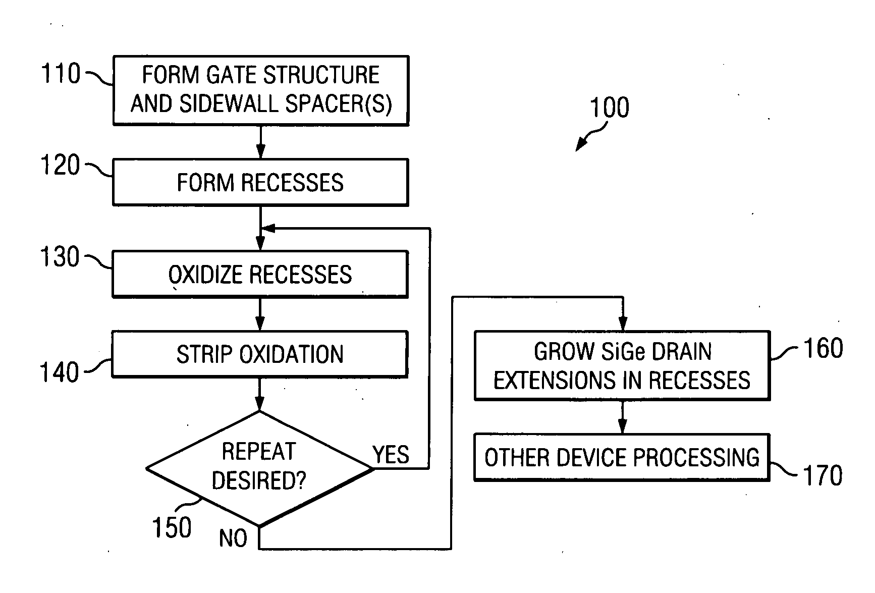
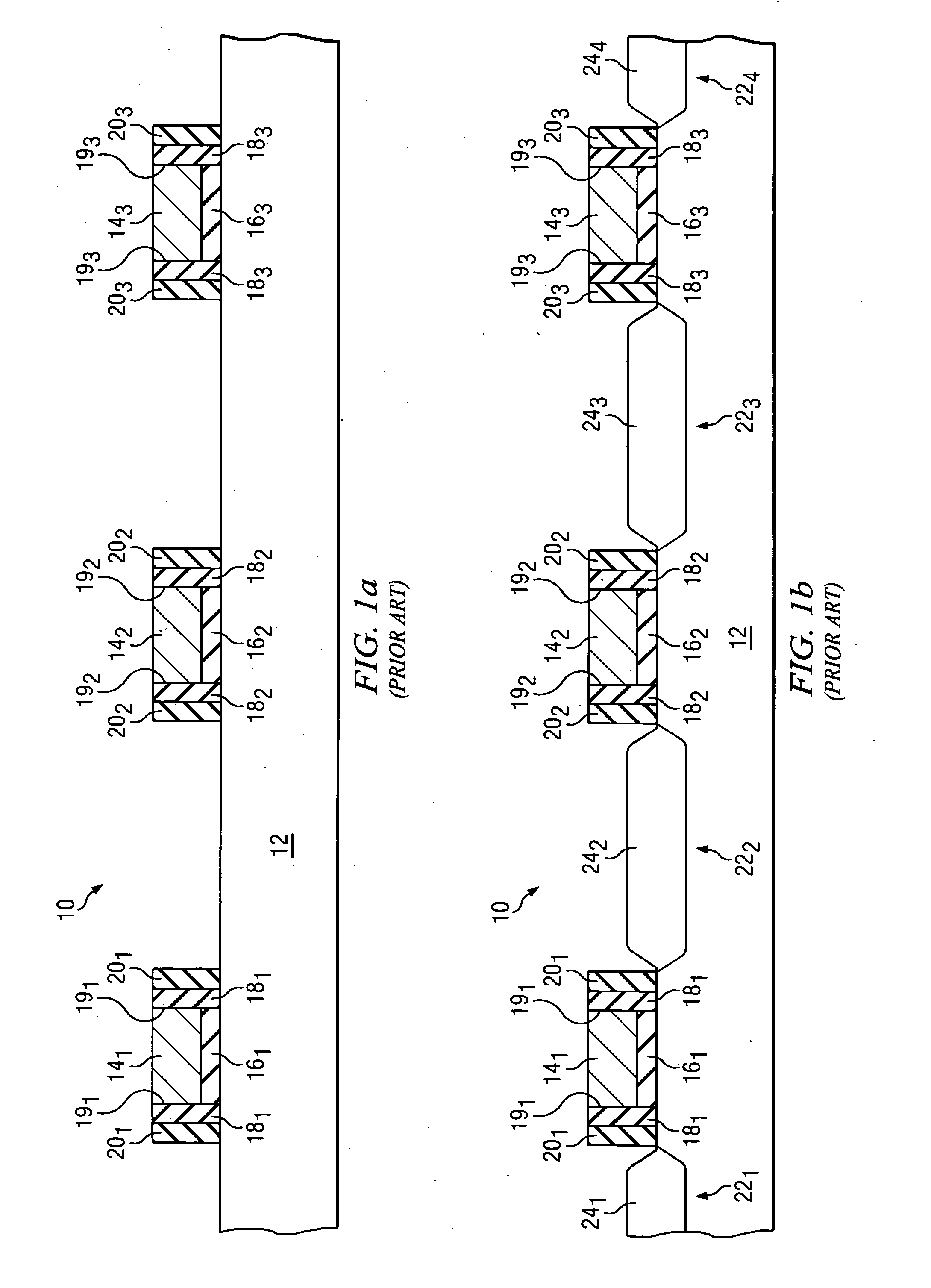
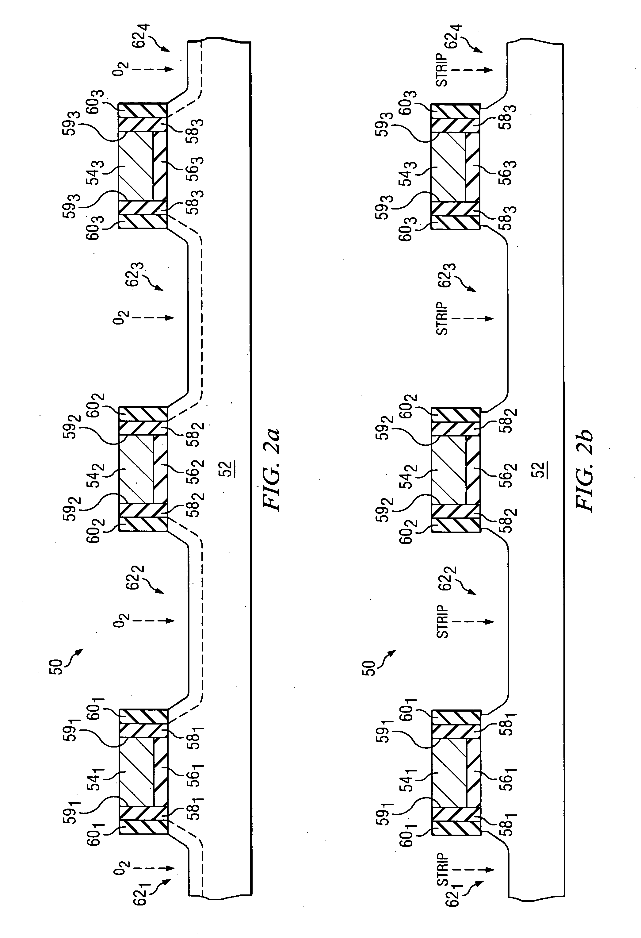
[0015]FIG. 1a illustrates a cross-sectional view of a prior art integrated circuit semiconductor device 10, where device 10 and the later discussion demonstrate in part the formation of recessed drain extensions according to the prior art. Device 10 is formed in connection with a silicon semiconductor substrate 12. Overlying substrate 12 are three gate conductors 141, 142, and 143, where typically each gate conductor 14x is formed at a same time and with a material such as polysilicon. Each gate conductor 14x is separated from substrate 12 by a respective gate insulator 161, 162, and 163, and the combination of conductor and respective gate insulator is sometimes referred to as a “gate stack.” Along each sidewall 19x of each gate conductor 14x is formed a first sidewall layer 18x, typically formed of an oxide, where often that oxide is grown on the sidewall 19x of the corresponding polysilicon gate structure. For example, with respect to gate 141, it has a first sidewall layer 181 f...


PUM


Abstract

A method of forming an integrated circuit transistor (50). The method provides a first semiconductor region (52) and forms (110) a gate structure (54x) in a fixed position relative to the first semiconductor region. The gate structure has a first sidewall and a second sidewall (59x). The method also forms at least a first layer (58x, 60x) adjacent the first sidewall and the second sidewall. The method also forms (120) at least one recess (62x) in the first semiconductor region and extending laterally outward from the gate structure. Additional steps in the method are first, oxidizing (130) the at least one recess such that an oxidized material is formed therein, second, stripping (140) at least a portion of the oxidized material, and third, forming (160) a second semiconductor region (66x) in the at least one recess.

Description

CROSS-REFERENCES TO RELATED APPLICATIONS [0001] Not Applicable. STATEMENT REGARDING FEDERALLY SPONSORED RESEARCH OR DEVELOPMENT [0002] Not Applicable. BACKGROUND OF THE INVENTION [0003] The present embodiments relate to electronic circuit manufacture and are more particularly directed to improving recessed drain extensions in a transistor device. [0004] Semiconductor devices are prevalent in all aspects of electronic circuits, and an often critical and dominant element used in such circuits is the transistor. Thus, due to the evolution of electronic design and its criteria, considerable effort has been made to improve transistor design. One approach currently being implemented involves creating so-called silicon strain in the transistor channel through the use of recessed silicon-germanium (SiGe) drain extensions. Generally, various steps occur in this context. First, a transistor gate stack is formed in a fixed relationship relative to a semiconductor substrate. Next, a portion or ...

Claims


Application Information

Patent Timeline
Patent Type & Authority Applications(United States)
IPC IPC(8): H01L29/772H01L21/336
CPCH01L21/823412H01L29/165H01L29/6656H01L29/66628H01L29/66636H01L29/7848
Inventor HALL, LINDSEY H.
Owner TEXAS INSTR INC
Features
  • R&D
  • Intellectual Property
  • Life Sciences
  • Materials
  • Tech Scout
  • Unparalleled Data Quality
  • Higher Quality Content
  • 60% Fewer Hallucinations
Learn More