Semiconductor device and method of manufacturing the same

a technology of semiconductors and semiconductors, applied in the direction of semiconductor devices, basic electric elements, electrical equipment, etc., can solve the problems of generating residues, difficult to shrink the device in the bit line direction, and difficulty in etching the device using the existing technology, so as to minimize the height of the gate in the memory cell, facilitate the process, and achieve the effect of high gate heigh

Inactive Publication Date: 2006-04-20
STMICROELECTRONICS SRL +1
View PDF5 Cites 10 Cited by
  • Summary
  • Abstract
  • Description
  • Claims
  • Application Information

AI Technical Summary

Benefits of technology

[0013] Accordingly, in view of the above problems, semiconductor device and method of manufacturing the same are disclosed in which a metal material of good electrical property and stress property is used as a barrier metal layer, a step between a memory cell form...

Problems solved by technology

A manufacturing method using the SAFG method can have the following problems.
First, the SAFG method is advantageous in the word line direction, but is disadvantageous in that it is difficult to shrink the device in a bit line direction because an existing RIE mode is used.
That is, in the process of etching the stack structure having a high step at the same time, which consists of Poly1/ONO/Poly2/WSi/Nitride/Oxynitride, etc., there is a difficulty in etching them using the existing technology if the design rule is small.
This process, however, is disadvantageous in that residues are generated because of by-products since several layers are etched at the same time and there is a limit to selection of chemicals for the p...

Method used


Image

  • Semiconductor device and method of manufacturing the same
  • Semiconductor device and method of manufacturing the same
  • Semiconductor device and method of manufacturing the same

Examples


Embodiment Construction

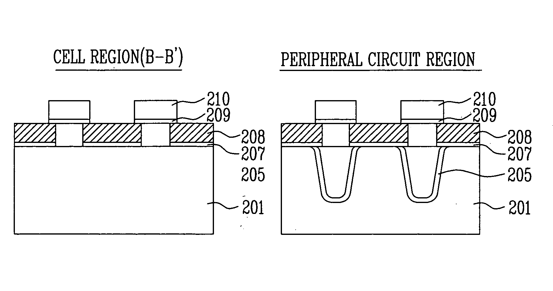
[0037] Now, the preferred embodiments will be described with reference to the accompanying drawings. Since preferred embodiments are provided for the purpose of explanation to those of ordinary skill in the art, they may be modified in various manners and the scope of this disclosure is not limited by the specific preferred embodiments described herein. Further, in the drawings, the thickness and size of each layer are exaggerated for convenience and clarity. Like reference numerals are used to identify the same or similar parts. Meanwhile, in case where it is stated that one film is “on” the other film or a semiconductor substrate, the one film may directly contact the other film or the semiconductor substrate. Or, one or more additional films may be disposed between the one film and the other film or the semiconductor substrate.

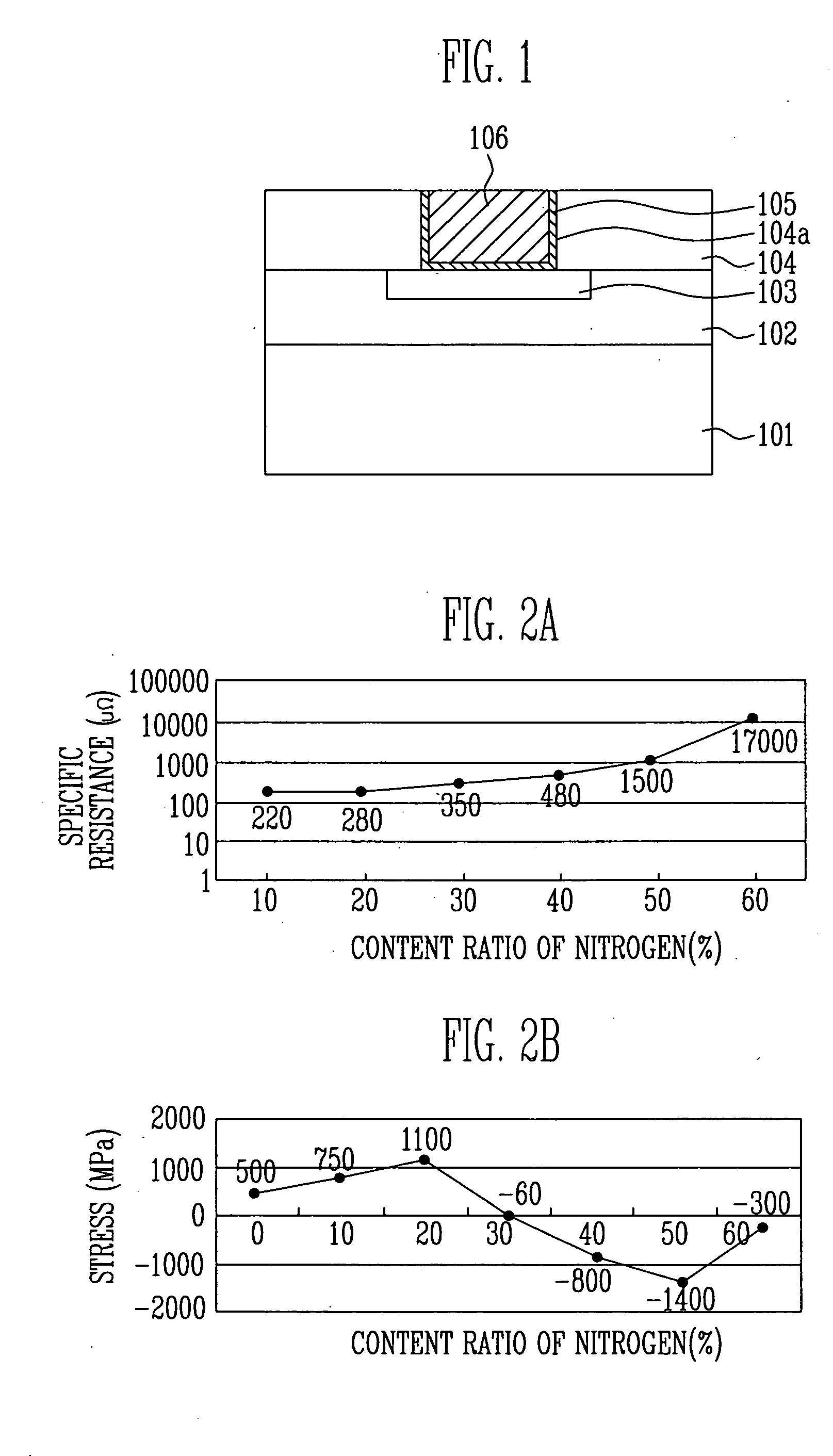
[0038]FIG. 1 is a sectional view illustrating a barrier metal layer of a disclosed semiconductor device.

[0039] Referring to FIG. 1, an interlayer insulat...


PUM


Abstract

Disclosed herein is a semiconductor device and method of manufacturing the same. A step between a memory cell formed in a cell region and a transistor formed in a peripheral circuit region is minimized, and the height of a gate in the memory cell is minimized. Accordingly, subsequent processes are facilitated and the electrical property of the device is thus improved.

Description

BACKGROUND [0001] 1. Technical Field [0002] A semiconductor device and method of manufacturing the same are disclosed in which the size of steps between memory cells and transistors can be reduced. [0003] 2. Description of the Related Art [0004] In a manufacture process of a NAND flash memory device, a SAFG (Self-Aligned Floating Gate) method is employed. This SAFG method is a technology where a tunnel oxide film and a polysilicon layer are sequentially formed on a semiconductor substrate portions of the polysilicon layer and the tunnel oxide film disposed in an element isolation region are then removed. The semiconductor substrate is then etched in a word line direction to form a trenches in the element isolation region. The trenches are then buried or filled with an insulating material to form an element isolation film while patterning the polysilicon layer. [0005] A manufacturing method using the SAFG method can have the following problems. [0006] First, the SAFG method is advant...

Claims


Application Information

Patent Timeline
IPC IPC(8): H01L21/336H01L29/76
CPCH01L27/105H01L27/11526H01L27/11543H01L29/42324H01L29/7842H10B41/40H10B41/48
Inventor JEONG, CHEOL MO
Owner STMICROELECTRONICS SRL
Why Eureka
Try Eureka