Flash gate stack notch to improve coupling ratio

a technology of flash memory and gate stack, which is applied in the direction of semiconductor flash memory cells, semiconductor devices, electrical devices, etc., can solve the problems of high cost, large difficulty in high density device packing, and short time required for reading data, etc., and achieve the effect of increasing the gate coupling ratio of a semiconductor flash memory cell

Inactive Publication Date: 2006-04-20
APPLIED MATERIALS INC
View PDF18 Cites 7 Cited by
  • Summary
  • Abstract
  • Description
  • Claims
  • Application Information

AI Technical Summary

Benefits of technology

[0017] The embodiments present invention generally relates a semiconductor flash memory device and a method of making the flash memory device with increased gate coupling ratio. In one embodiment, a semiconductor flash memory device comprises a semiconductor substrate, a tunneling dielectric film formed on said semiconductor substrate, a first gate film and a second gate film on said tunneling film, wherein the first gate film is adjacent and on top of the tunneling film and the second gate film is on top of the first gate film, the first gate film has notches at the interface with the tunneling dielectric film and at the edge of the device, and the heights of the notches are smaller than the thickness of the first gate film, and an interlayer dielectric film between said first gate film and said second gate film.
[0018] In another embodiment, a method of increasing the gate coupling ratio of a semiconductor flash memory cell comprises depositing a tunneling dielectric film on said semiconductor substrate, depositing a first gate film on said tunneling dielectric film, depositing an interlayer dielectric film on said first gate film, depositing a second gate film on said interlayer dielectric film, patterning the semiconductor substrate after the second gate film is deposited, etching the second gate film and the interlayer dielectric film, etching the first gate film to leave notches at the interface with the tunneling dielectric film and at the edge of the device, and etching the tunneling dielectric film.

Problems solved by technology

Then, a high electric field is created at the drain end of the channel, heating the electrons and causing avalanching.
Thus, the time required for reading the data can be relatively short.
But, increasing the cell size causes a great difficulty in high density device packing.
As a result, the conventional flash has problems in that they consume high power and are less reliable for effective programming.

Method used


Image

  • Flash gate stack notch to improve coupling ratio
  • Flash gate stack notch to improve coupling ratio
  • Flash gate stack notch to improve coupling ratio

Examples


Embodiment Construction

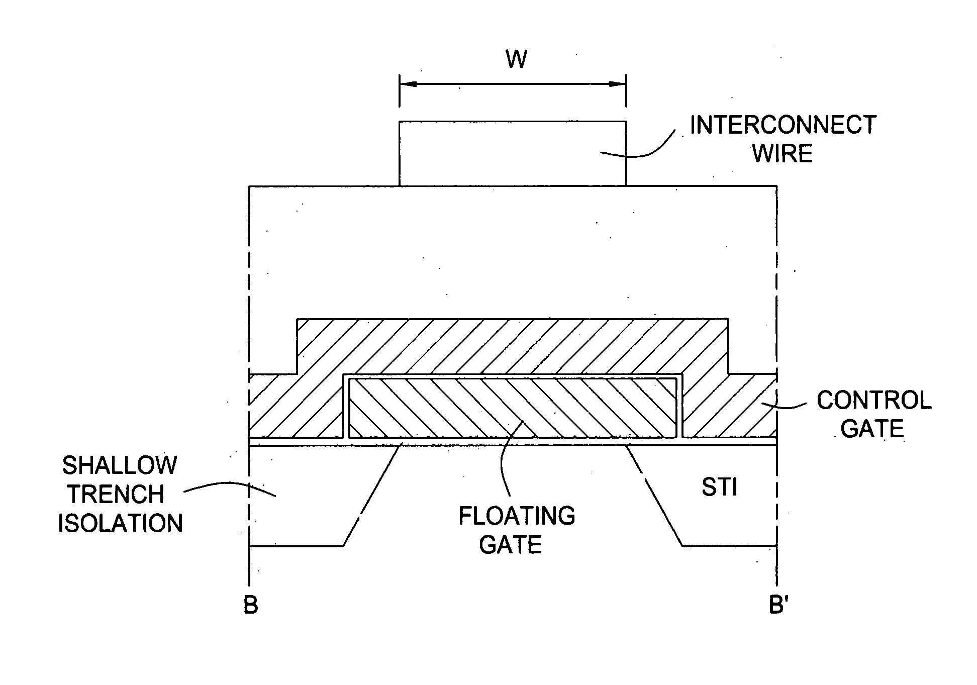
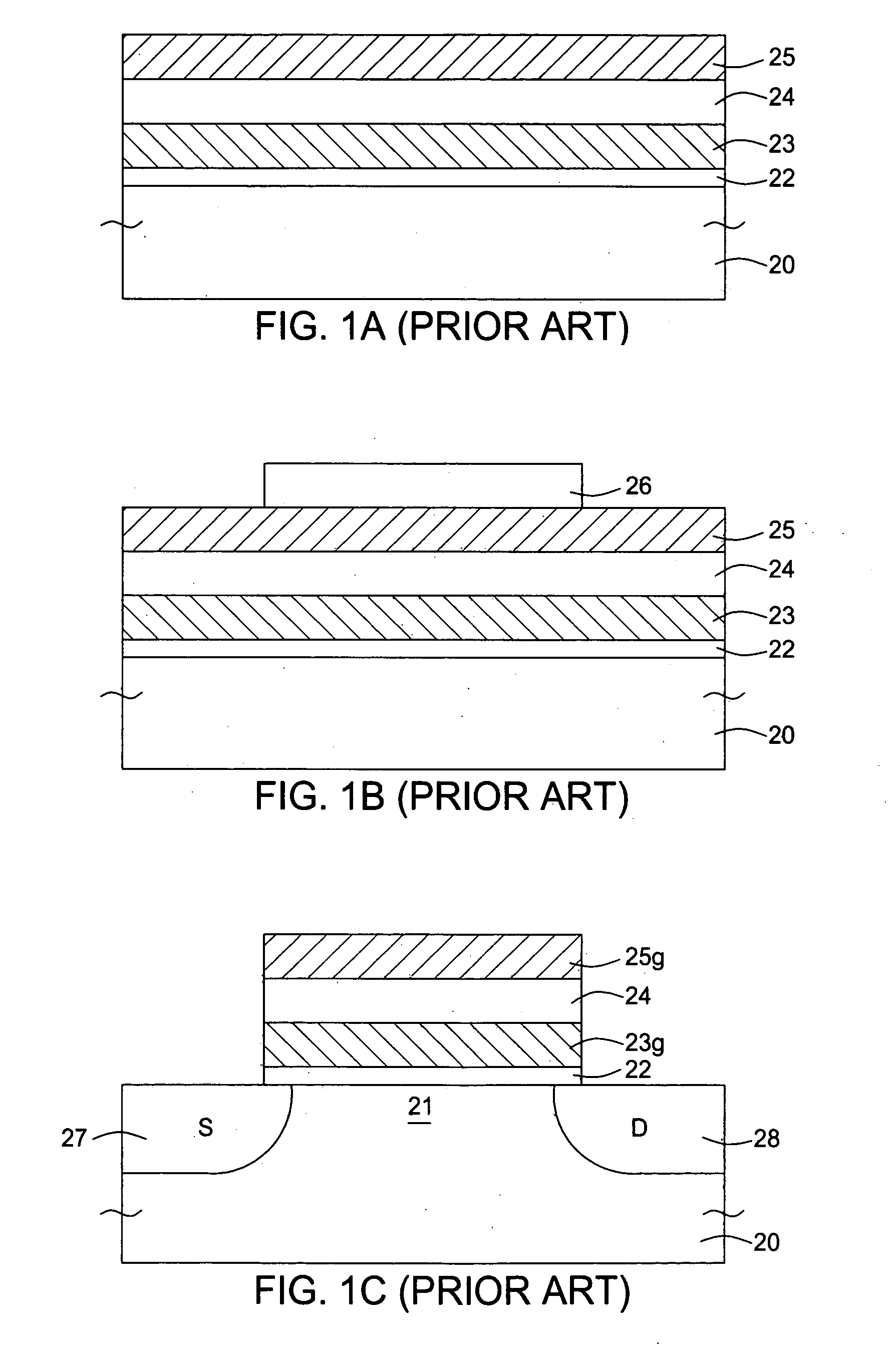
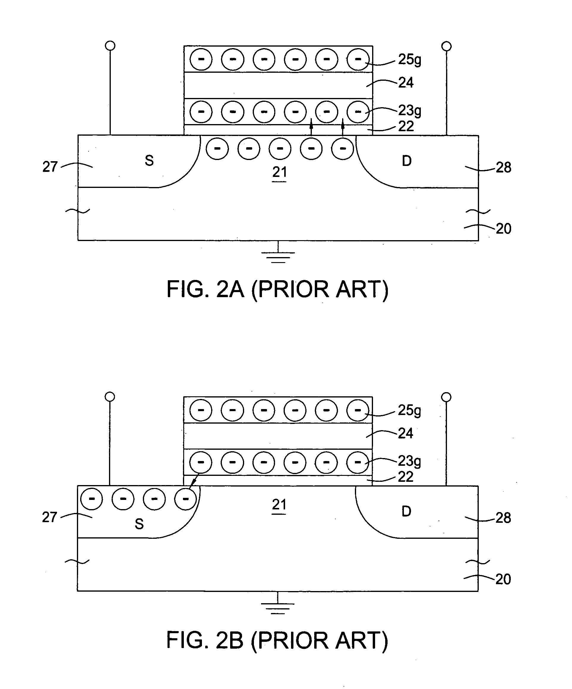
[0028] The embodiments present invention generally relates a semiconductor flash memory device and a method of making the flash memory device with increased gate coupling ratio.

[0029] As described earlier, gate coupling ratio can be increased by either increasing Ccg or reducing other capacitances, such as Cfs, Cfw, Cfd, and Cmos. Typically, Cfs, Cfw and Cfd are much smaller (cg and Cmos. Increasing Ccg or decreasing Cmos would have larger impacts in increasing gate coupling ratio (CR), compared to decreasing Cfs, Cfw or Cfd.

[0030] Ccg is the capacitance between the control polysilicon gate and the floating silicon gate. It is a function of the surface area of the interlayer oxide (AILO) between the control polysilicon gate and the floating polysilicon gate, and interlayer oxide thickness (tILO) as shown in equation (2).

Ccg=εILOAILO / tILO  (2)

Where, εILO is the dielectric constant of the interlayer oxide (ILO).

[0031] Ccg can be increased by increasing εTNO or ATNO, or by decrea...


PUM


Abstract

A semiconductor flash memory device with increased gate coupling ratio and a method of preparing this flash memory device. The semiconductor flash memory device includes a notched floating polysilicon gate. The notches are at the interface between the floating polysilicon layer and the tunneling dielectric layer. The notches reduce the capacitance between the floating polysilicon and the channel region. The reduced capacitance results in the increased gate coupling ratio. The degree of capacitance reduction, which affects the gate coupling ratio increase, is controlled by the width of the notches. The floating polysilicon gate etch includes a first anisotropic etch and a second isotropic etch. The widths of the notches are controlled by the etch time of the isotropic etch.

Description

BACKGROUND OF THE INVENTION [0001] 1. Field of the Invention [0002] Embodiments of the present invention generally relate to a semiconductor flash memory device and a method for the semiconductor flash memory device. More particularly, the embodiments of the present invention relate to a flash memory device and a method of making the device with increased coupling ratio compared to the conventional flash memory device. [0003] 2. Description of the Related Art [0004] Memory devices are largely divided into volatile memory devices, which lose data when power is removed, and non-volatile memory devices, in which the stored information is retained without external power. For non-volatile memory devices, there are read-only memories (ROMs), erasable programmable ROMs (EPROMs) and electrically erasable programmable ROMs (EEPROMs). [0005] Among the non-volatile memory devices, the ROMs are devices in which programming is done during manufacturing by a masking step. The EPROMs and EEPROMs a...

Claims


Application Information

Patent Timeline
Patent Type & Authority Applications(United States)
IPC IPC(8): H01L29/788
CPCH01L21/28273H01L29/42324H01L29/40114
Inventor SMAYLING, MICHAEL C.
Owner APPLIED MATERIALS INC
Why Eureka
Try Eureka