Variable resistance device made of a material which has an electric resistance value changing in accordance with an applied electric field and maintains the electric resistance value after being changed in a nonvolatile manner, and a semiconductor apparatus including the same

Inactive Publication Date: 2006-04-20
PANASONIC CORP
View PDF1 Cites 40 Cited by
  • Summary
  • Abstract
  • Description
  • Claims
  • Application Information

AI Technical Summary

Benefits of technology

[0025] The semiconductor apparatus of the present invention with the above structure includes a variable resistance device in which the control electrodes and the data path are separated from each other. Consequently, the semiconductor of the present invention is capable of (1) ensuring reliable detection of changes in the electric properties created by applying an electric field, and (2) providing high flexibility in the designing by reducing the limitations of the electronic circuit.
[0026] The present i

Problems solved by technology

However, since the electrodes 52A and 52B applying a voltage pulse to the variable resistance layers 523 are also used as the data paths, the above-mentioned conventional technology

Method used


Image

  • Variable resistance device made of a material which has an electric resistance value changing in accordance with an applied electric field and maintains the electric resistance value after being changed in a nonvolatile manner, and a semiconductor apparatus including the same
  • Variable resistance device made of a material which has an electric resistance value changing in accordance with an applied electric field and maintains the electric resistance value after being changed in a nonvolatile manner, and a semiconductor apparatus including the same
  • Variable resistance device made of a material which has an electric resistance value changing in accordance with an applied electric field and maintains the electric resistance value after being changed in a nonvolatile manner, and a semiconductor apparatus including the same

Examples


embodiment 1

1. Embodiment 1

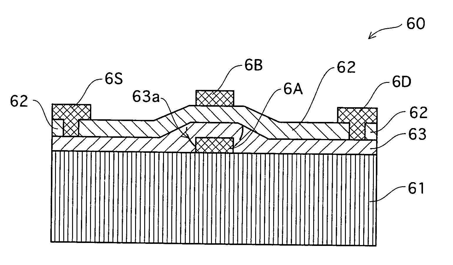
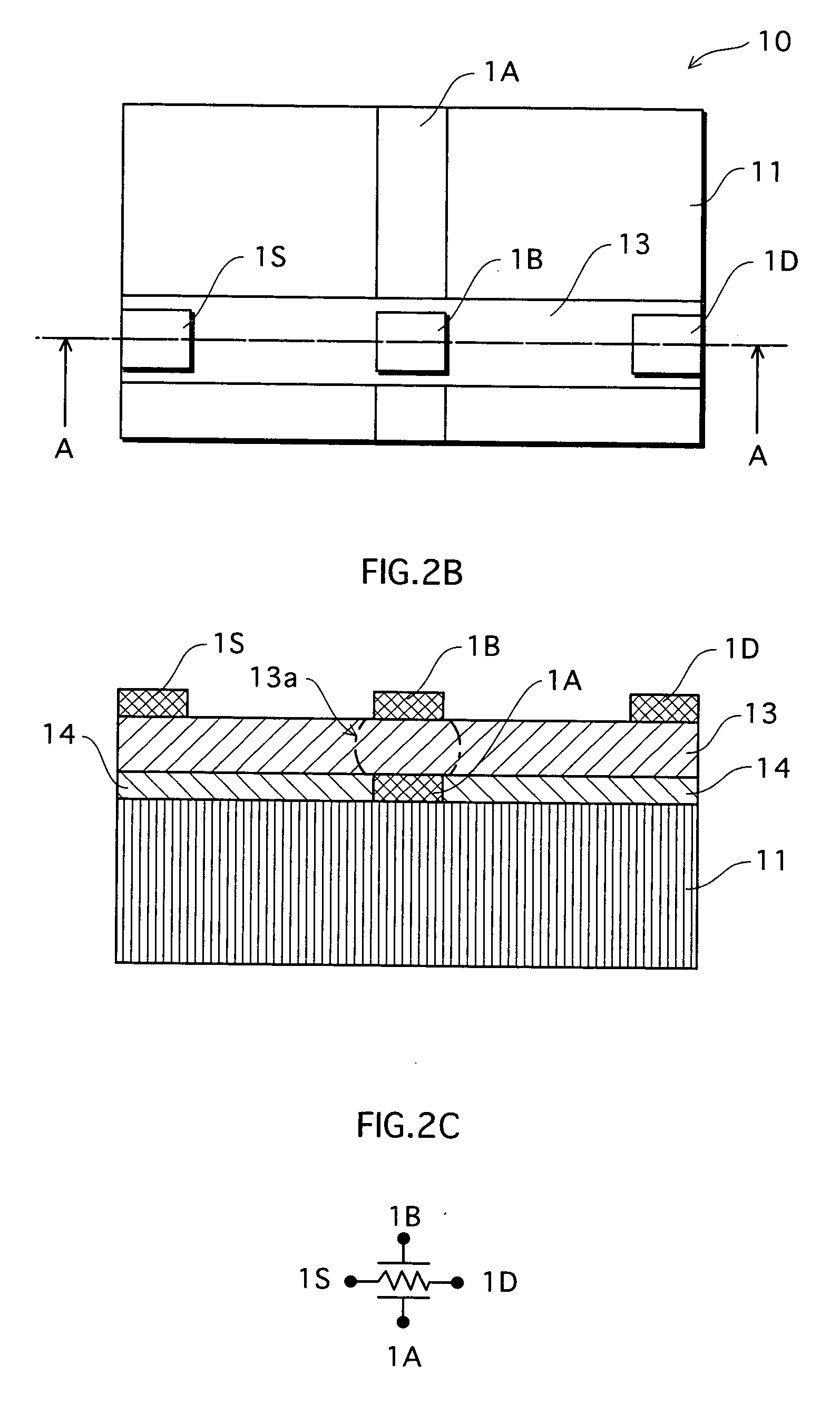
[0074] A variable resistance device 10 according to Embodiment 1 is described below in reference to FIGS. 2A to 2C. FIG. 2A is a plain view showing relevant parts of the variable resistance device 10; FIG. 2B is a schematic cross section of the variable resistance device 10 along the line A-A; and FIG. 2C is an equivalent circuit diagram of the variable resistance device 10.

1.1 Structure of Variable Resistance Device 10

[0075] The variable resistance device 10 has a layered structure in which a 1st electrode 1A and a planarizing layer (for example, a silicon oxide layer) 14 are formed on the main surface of a substrate (for example, a silicon substrate) 11, and a variable resistance layer 13 is formed on top of the 1st electrode 1A and planarizing layer 14, as shown in FIGS. 2A and 2B. On the surface of the variable resistance layer 13, a 2nd electrode 1B, a 3rd electrode 1S and a 4th electrode 1D are formed. As shown in FIG. 2A, the 3rd, 2nd and 4th electrodes 1S, 1...

modification 1

[Modification 1]

[0093] A variable resistance device 20 according to Modification 1 is described next in reference to FIGS. 3A and 3B.

[0094] As shown in FIG. 3A, the variable resistance device 20 according to the present modification differs from the above-mentioned variable resistance device 10 in the positions of 3rd and 4th electrodes 2S and 2D composing a read electrode pair, and this is a characteristic feature of the variable resistance device 20. In the variable resistance device 20, the 3rd and 4th electrodes 2S and 2D are formed on top of a substrate (e.g. a silicon substrate) 21 along with a 1st electrode 2A, and a planarizing layer (e.g. a silicon oxide layer) 24 is formed to fill the space between the 3rd and 1st electrodes 2S and 2A and between the 1st and 4th electrodes 2A and 2D. Formed on top of the electrodes 2S, 2A and 2D and the planarizing layer 24 is a variable resistance layer 23, on which only a 2nd electrode 2B is superimposed. As a constituent material of th...

modification 2

[Modification 2]

[0099] A variable resistance device 30 according to Modification 2 is described next in reference to FIGS. 4A and 4B.

[0100] As shown in FIG. 4A, the variable resistance device 30 according to the present modification has the same positioning and structure as the variable resistance device 10 of Embodiment 1 in terms of a 1st electrode 3A formed on a substrate 31, a planarizing layer 34, a variable resistance layer 33, 2nd and 3rd electrodes 3B and 3S. The variable resistance device 30 of the present modification differs from the above variable resistance device 10 in the position of a 4th electrode 3D.

[0101] In the variable resistance device 30 of the present modification, the 4th electrode 3D is positioned between the substrate 31 and the variable resistance layer 33, as with the 4th electrode 2D of Modification 1 above. In the horizontal direction in FIG. 4A, the 3rd electrode 3S is positioned to the left of the 2nd electrode 3B on the surface of the variable res...


PUM


Abstract

The variable resistance device of the present invention comprises a variable resistance layer. The variable resistance layer is made of a material which has an electric resistance changing in accordance with an applied electric field and maintains the electric resistance after being changed in a nonvolatile manner. Provided for the variable resistance layer are four electrodes independent of each other. Of them, two electrodes constitute a control electrode pair, while the remaining two electrodes constituting a read electrode pair. The controle electrode pair is formed for applying an electric field to the variable resistance layer. On the other hand, the read electrode pair is formed as a data path making use of changes in the electric resistance.

Description

BACKGROUND OF THE INVENTION [0001] [1] Field of the Invention [0002] The present invention relates to: a variable resistance device made of a material which has an electric resistance changing in accordance with an applied electric field and maintains the electric resistance after being changed in a nonvolatile manner; and a semiconductor apparatus including the variable resistance device, and in particular relates to the electrode structure of the variable resistance device. [0003] [2] Related Art [0004] Materials having a perovskite structure, especially colossal magnetoresistive (CMR) materials, have electric properties changing due to the influence of external factors such as a magnetic field. Research and development for applying such materials to electronic apparatuses are being carried out. One example of such CMR materials is Pr0.7Ca0.3MnO3 (referred to hereinafter as “PCMO”), and the electric properties of this can be changed by applying a pulse once or more. [0005] In conv...

Claims


Application Information

Patent Timeline
IPC IPC(8): H01L29/00H01L29/76
CPCG11C13/0007G11C19/00G11C2213/31G11C2213/52H01L45/06H01L45/1206H01L45/122H01L45/145H01L45/147H03K19/17736H03K19/1776H03K19/1778H10N70/253H10N70/821H10N70/20H10N70/8836H10N70/883
Inventor WEI, ZHIQIANGKATO, YOSHIHISA
Owner PANASONIC CORP
Why Eureka
Try Eureka