Voltage detection circuit
a voltage detection and circuit technology, applied in pulse manipulation, pulse technique, instruments, etc., can solve the problems of increasing chip area, increasing power consumption, and uncertain operation of cmos inverter circuits
- Summary
- Abstract
- Description
- Claims
- Application Information
AI Technical Summary
Benefits of technology
Problems solved by technology
Method used
Image

Examples
Embodiment Construction
[0045] From the descriptions of the specification and accompanying drawings, at least following subjects become apparent.
[0046] ===Configuration of Voltage Detection Circuit===
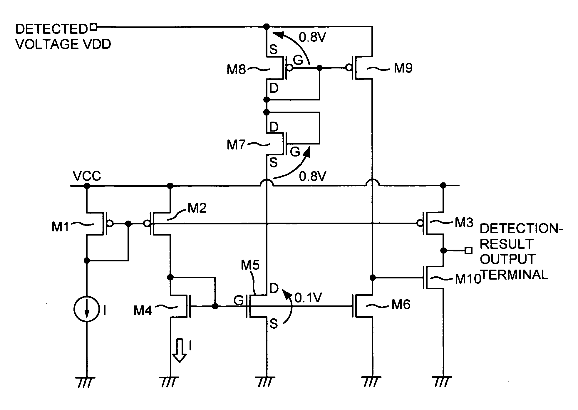
[0047]FIG. 1 is a circuit diagram showing an example of a configuration of a voltage detection circuit according to an implementation of the present invention.
[0048] The voltage detection circuit shown in the figure is a voltage detection circuit detecting that a voltage VDD (“detected voltage”) becomes lower than 1.7 V, and is provided with P-channel type MOSFET (hereinafter, referred to as PMOS) M1, M2, M3, M8 and M9, N-channel type MOSFET (hereinafter, referred to as NMOS) M4, M5, M6 and M7 and a constant-current circuit I.
[0049] The voltage detection circuit shown in FIG. 1 is integrated with a logic circuit whose power supply voltage is the voltage VDD, on the same chip, for example.
[0050] It is assumed that transistor size ratios (W / L) are equal for W (gate width) and L (gate length) of the PMOS M1, ...
PUM
 Abstract
Description
Claims
Application Information
 - R&D
- Intellectual Property
- Life Sciences
- Materials
- Tech Scout
- Unparalleled Data Quality
- Higher Quality Content
- 60% Fewer Hallucinations
Browse by: Latest US Patents, China's latest patents, Technical Efficacy Thesaurus, Application Domain, Technology Topic, Popular Technical Reports.
© 2025 PatSnap. All rights reserved.Legal|Privacy policy|Modern Slavery Act Transparency Statement|Sitemap|About US| Contact US: help@patsnap.com