Method for minimizing the translation overhead for large I/O transfers

a technology for large i/o transfers, applied in the field of minimizing the translation overhead for large i/o transfers, can solve problems such as affecting i/o throughput, and achieve the effects of reducing the overall wait time for accessing the address-mapping table, reducing the additional time, and increasing the i/o response tim

Inactive Publication Date: 2006-04-20
IBM CORP
View PDF6 Cites 7 Cited by
  • Summary
  • Abstract
  • Description
  • Claims
  • Application Information

AI Technical Summary

Benefits of technology

[0006] In the present invention, advantage is taken of the fact that the latency time necessary to call the mapping program to resolve a single address is almost the same as the time to call the program to resolve a number of addresses. For example, when a 128-byte cache line is used to send 8-byte I / O addresses, sixteen addresses are present; the addresses for all sixteen pages can be resolved with minimal additional time over the cost of resolving one of the addresses. In order to take advantage of this fact, the inventive process requires that system memory, which is generally allocated in pages of 4 kilobytes, be allocated in blocks of n pages, with n being the number of device addresses that can be stored in a cache line. With larger blocks of memory being allocated, the driver can initiate the copying of n pages into system memory with a single call to the address-mapping program. In a cache line that can hold sixteen addresses, memory would be allocated in 64-kilobyte blocks and sixteen 4-kilobyte pages can be copied before another call to the address-mapping program. The overall wait time for accessing the address-mapping table is thus reduced, increasing I / O response time. No change is required to the pagination in the operating system, which can continue to operate on 4-kilobyte pages. All changes are made in the hardware mapping programs and in the device driver software.

Problems solved by technology

Because it is necessary to call the mapping program to map the address, undesirable latencies are introduced into the DMA process, impacting I / O throughput.

Method used


Image

  • Method for minimizing the translation overhead for large I/O transfers
  • Method for minimizing the translation overhead for large I/O transfers
  • Method for minimizing the translation overhead for large I/O transfers

Examples


Embodiment Construction

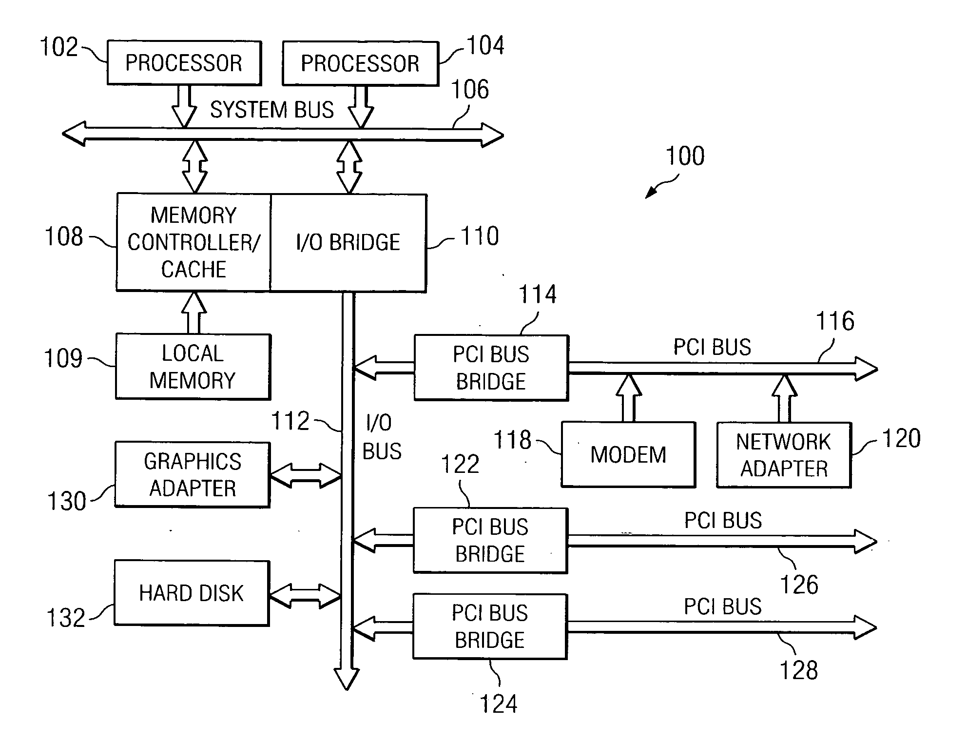
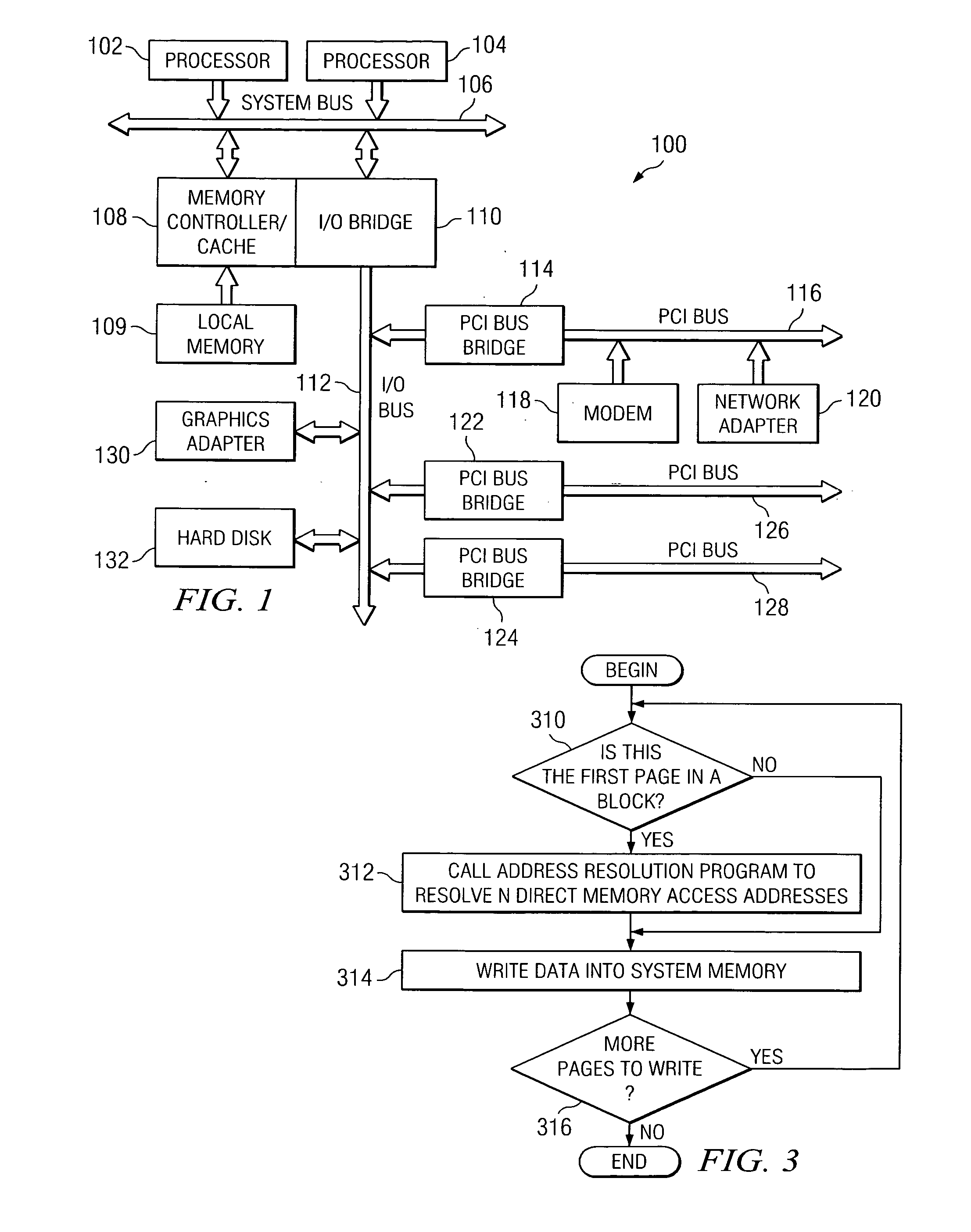
[0013] Referring now to FIG. 1, a block diagram of a data processing system is depicted in accordance with a preferred embodiment of the present invention. Data processing system 100 may be a symmetric multiprocessor (SMP) system including a plurality of processors 102 and 104 connected to system bus 106. Alternatively, a single processor system may be employed. Also connected to system bus 106 is memory controller / cache 108, which provides an interface to local memory 109. I / O bus bridge 110 is connected to system bus 106 and provides an interface to I / O bus 112. Memory controller / cache 108 and I / O bus bridge 110 may be integrated as depicted.

[0014] Peripheral component interconnect (PCI) bus bridge 114 connected to I / O bus 112 provides an interface to PCI local bus 116. A number of modems may be connected to PCI local bus 116. Typical PCI bus implementations will support four PCI expansion slots or add-in connectors.

[0015] Additional PCI bus bridges 122 and 124 provide interface...


PUM


Abstract

A number of DMA addresses are resolved to system memory addresses at a time to decrease latency time. The number of addresses resolved at a time is preferably correlated to the number of DMA addresses that can be stored in a single cache line. Additionally, system memory is allocated in larger blocks that can store all of the information from the DMA addresses in a cache line. No change is required to the operating system, which can continue to operate on the page size it is set for. All changes are made in the hardware mapping programs and in the device driver software.

Description

BACKGROUND OF THE INVENTION [0001] 1. Technical Field [0002] This application relates to managing addressing and memory sharing between the operating system and I / O device drivers performing direct memory access to system memory. [0003] 2. Description of Related Art [0004] Direct Memory Access (DMA) is a hardware mechanism that allows peripheral components to transfer their I / O data directly to and from main memory without the need for the system processor to be involved in the transfer. Use of this mechanism can greatly increase throughput to and from a device, because a great deal of overhead is eliminated. A device driver will set up the DMA transfer and synchronize with the hardware, which actually performs the transfer. In this process, the device driver must provide an interface between devices that use 32-bit physical addresses and system code that uses 64-bit virtual addresses. DMA operations call an address-mapping program to map device page addresses to physical memory. Ta...

Claims


Application Information

Patent Timeline
Patent Type & Authority Applications(United States)
IPC IPC(8): G06F13/28
CPCG06F12/1081G06F13/28
Inventor BUCKLAND, PATRICK ALLENHUA, BINH K.KODUKULA, SIVARAMA K.
Owner IBM CORP
Why Eureka
Try Eureka