

Integrated circuit selective scaling
a selective scaling and integrated circuit technology, applied in the field of integrated circuit design, can solve the problems of simple linear geometric scaling (i.e., multiplying), insufficient post-layout modifications alone to achieve the desired yield improvement, and insufficient yield improvement, etc., to achieve the effect of improving the yield of the integrated circuit design layout and improving yield
- Summary
- Abstract
- Description
- Claims
- Application Information
AI Technical Summary
Benefits of technology
Problems solved by technology
Method used
Image

Examples
Embodiment Construction
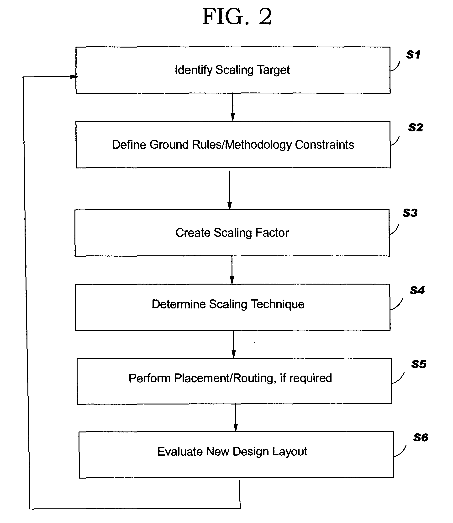
[0021] For purposes of organization only, the description includes the following headings: I. System Overview, II. Operational Methodology, III. Conclusion.
[0022] I. System Overview
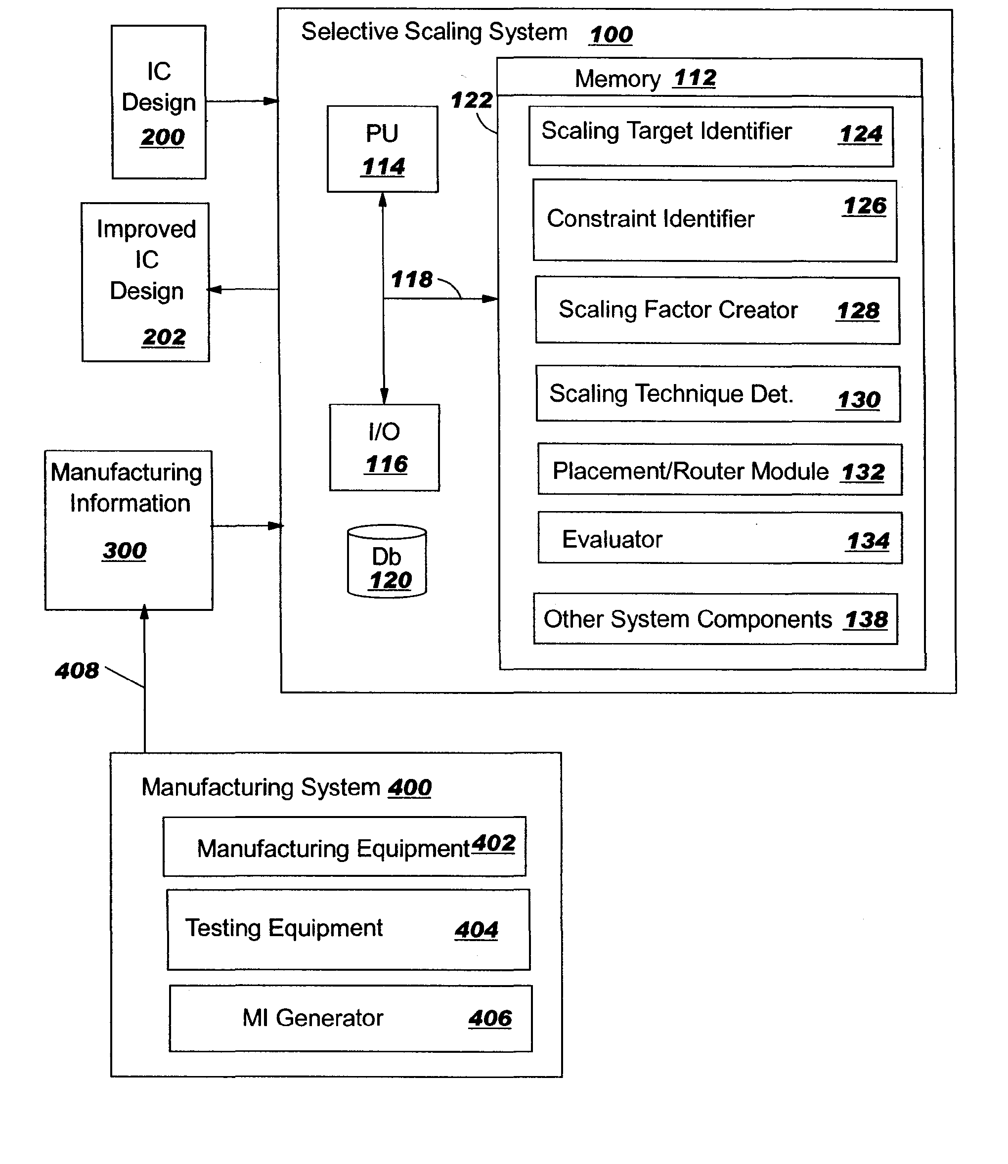
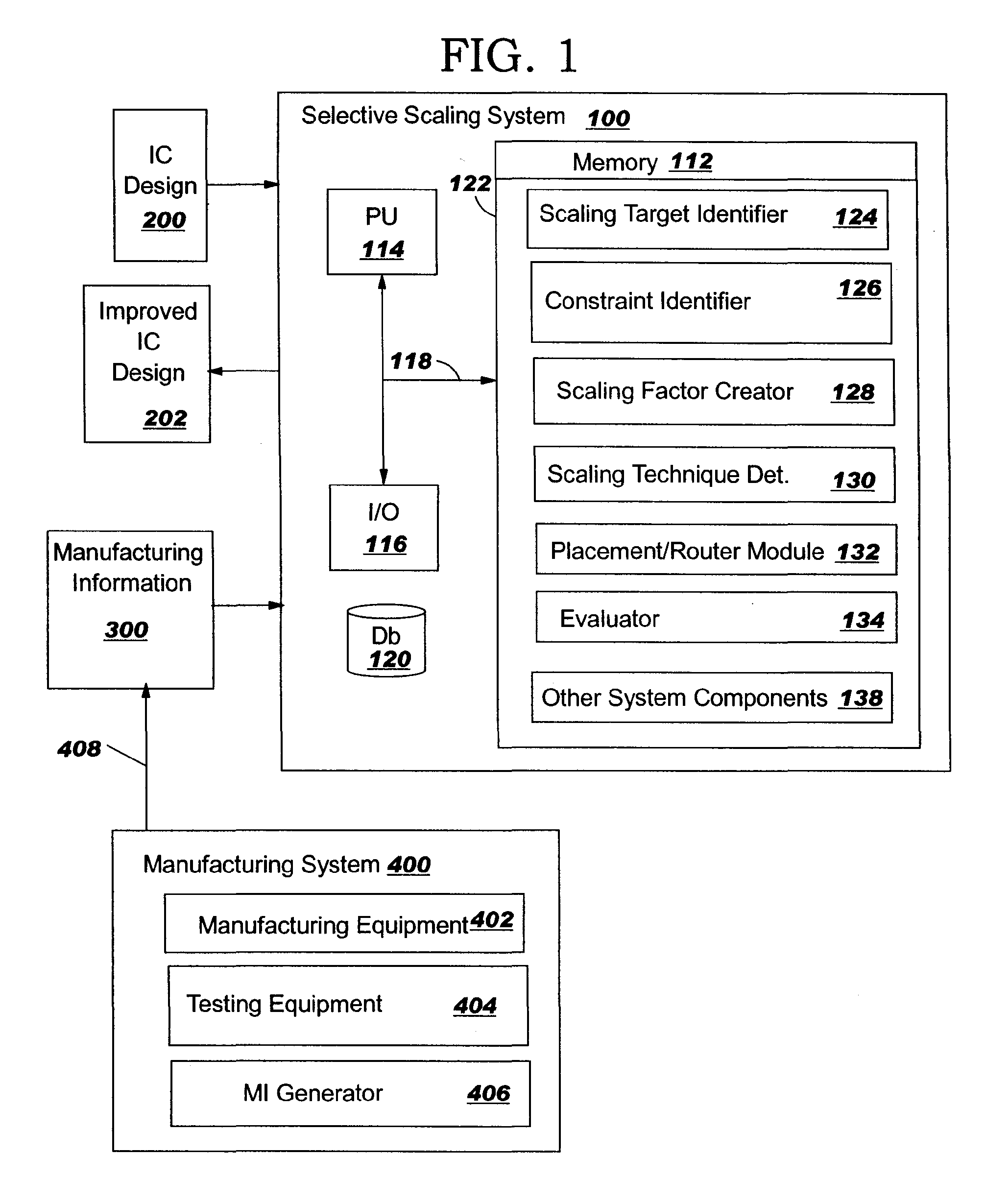
[0023] With reference to the accompanying drawings, FIG. 1 is a block diagram of an integrated circuit (IC) design selective scaling system 100 according to one embodiment of the invention. System 100 includes a memory 112, a processing unit (PU) 114, input / output devices (I / O) 116 and a bus 118. A database 120 may also be provided for storage of data relative to processing tasks. Memory 112 includes a program product 122 that, when executed by PU 114, comprises various functional capabilities described in further detail below. Memory 112 (and database 120) may comprise any known type of data storage system and / or transmission media, including magnetic media, optical media, random access memory (RAM), read only memory (ROM), a data object, etc. Moreover, memory 112 (and database 120) may reside at a sin...
PUM
 Abstract
Description
Claims
Application Information