Iridium oxide nanowires and method for forming same

a technology of iridium oxide nanowires and nanowires, which is applied in the direction of crystal growth process, polycrystalline material growth, chemically reactive gas growth, etc., can solve the problems of no process that is able to form or template metallic nanowires without the use of porous material forms or templates, and add a considerable degree of complexity to the process, etc., to achieve good crystallinity and electrical properties, high aspect ratio iro2

Inactive Publication Date: 2006-04-27
SHARP KK
View PDF1 Cites 47 Cited by
  • Summary
  • Abstract
  • Description
  • Claims
  • Application Information

AI Technical Summary

Benefits of technology

[0010] This application describes IrO2 nanowires grown on Ti, TiN, TaN and SiO2 substrates. The growth length, density, and vertical orientation can be controlled by the choice of temperature, pressure, flow, substrate material, and time. Variations in the deposition process permit a very high aspect ratio IrO2 nano wire to be grown, with a diameter of only 10-50 nanometers (nm), and a length as great as 1-2 um (microns). The nanowires obtained have good crystallinity and electrical properties.

Problems solved by technology

However, no processes have been reported that are able to form metallic nanowires without the use of porous material forms or templates.
The templates add a considerable degree of complexity to the process.
The crystalline structure is a result of defects, or a high dislocation density, resulting from the fact that there is insufficient diffusion to overcome the effects of shadowing during growth, which acts to provide more precursor to the nanorod tips than to the nanorod stem, or rod bottom sections.

Method used


Image

  • Iridium oxide nanowires and method for forming same
  • Iridium oxide nanowires and method for forming same
  • Iridium oxide nanowires and method for forming same

Examples


Embodiment Construction

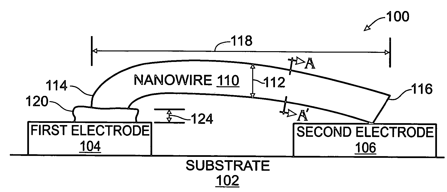
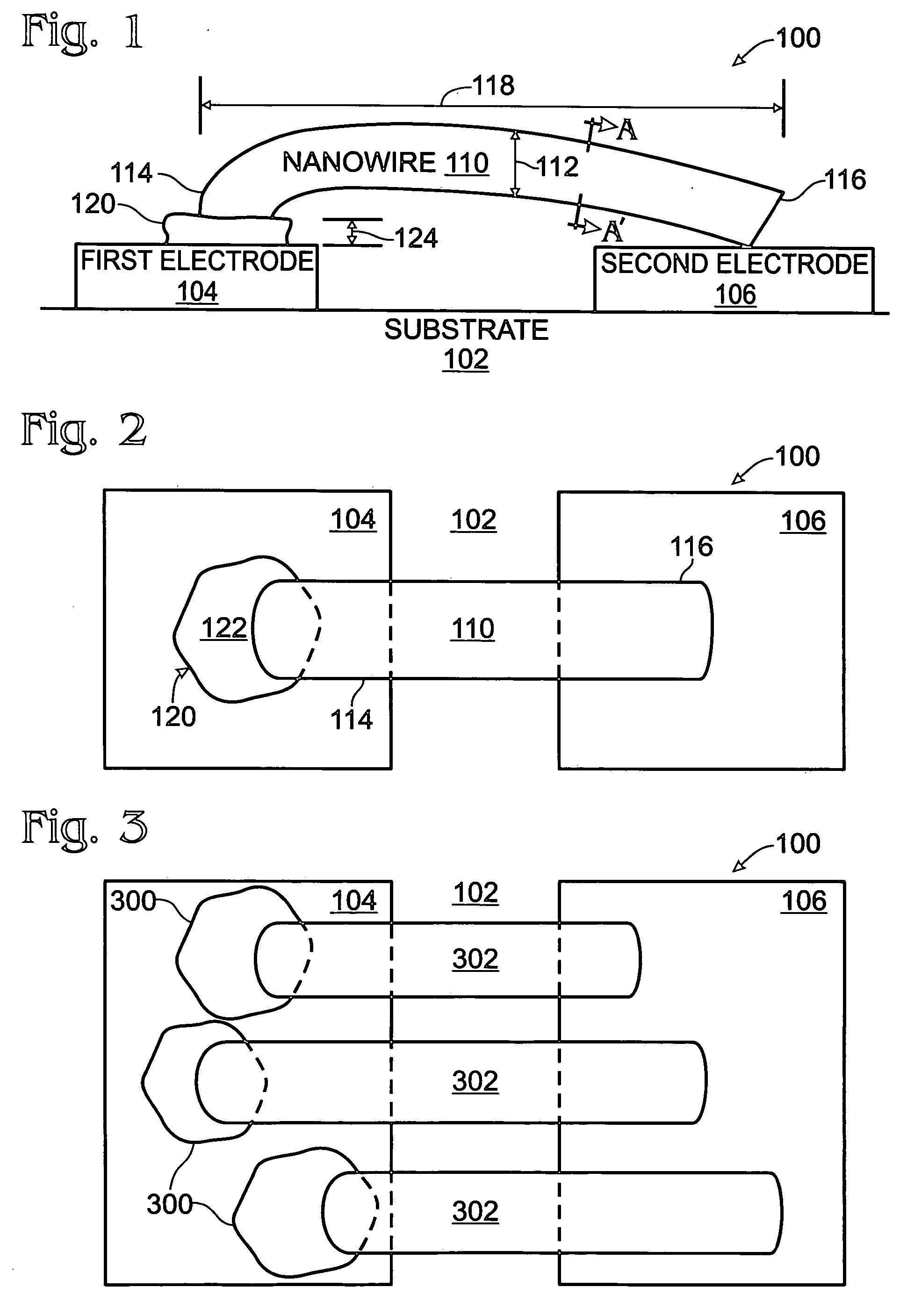
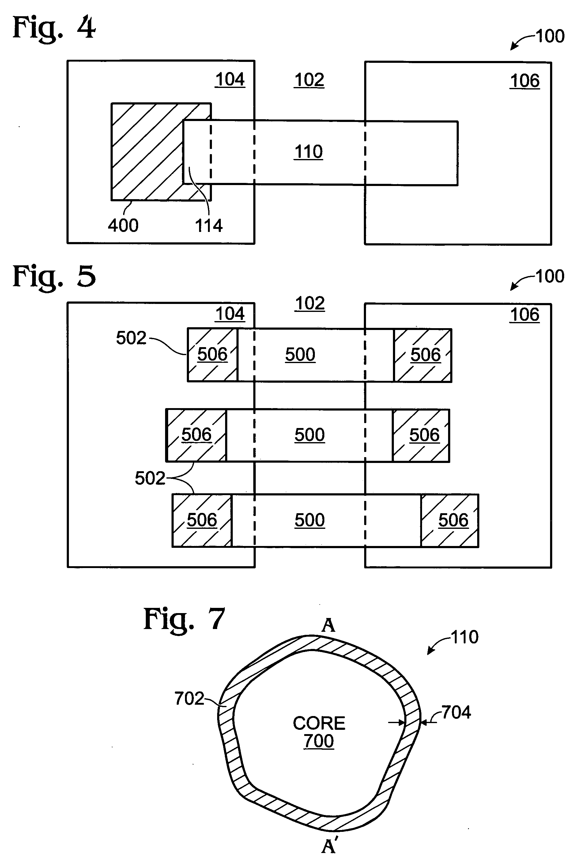
[0028]FIG. 1 is a partial cross-sectional view of an iridium oxide (IrOx) nanowire electrical interconnection. The electrical interconnection 100 comprises a substrate 102, such as silicon or silicon oxide. A first electrically conductive electrode 104 and a second electrically conductive electrode 106 are formed on the substrate 102. The electrode material can be any conventional IC fabrication metal, metal oxide, or conductive semiconductor material. For example, the first and second electrodes 104 / 106 may be Ti, Co, Ni, Au, Ta, poly-Si, SiGe, Pt, Ir, TiN, or TaN.

[0029] An IrOx nanowire 110, with a diameter 112 of less than 1000 Å, has a proximal end 114 connected to the first electrode 104 and a distal end 116 connected to the second electrode 106. The value of “x” may be 2, in which case the Ir is completely oxidized, to values approaching zero, in which case the Ir is incompletely oxidized. In some aspects, the IrOx nanowire 110 has a diameter 112 in the range of 100 to 1000 Å...


PUM

PropertyMeasurementUnit
thicknessaaaaaaaaaa
pressureaaaaaaaaaa
lengthaaaaaaaaaa

Abstract

Iridium oxide (IrOx) nanowires and a method forming the nanowires are provided. The method comprises: providing a growth promotion film with non-continuous surfaces, having a thickness in the range of 0.5 to 5 nanometers (nm), and made from a material such as Ti, Co, Ni, Au, Ta, polycrystalline silicon (poly-Si), SiGe, Pt, Ir, TiN, or TaN; establishing a substrate temperature in the range of 200 to 600 degrees C.; introducing oxygen as a precursor reaction gas; introducing a (methylcyclopentadienyl)(1,5-cyclooctadiene)iridium(I) precursor; using a metalorganic chemical vapor deposition (MOCVD) process, growing IrOx nanowires from the growth promotion film surfaces. The IrOx nanowires have a diameter in the range of 100 to 1000 Å, a length in the range of 1000 Å to 2 microns, an aspect ratio (length to width) of greater than 50:1. Further, the nanowires include single-crystal nanowire cores covered with an amorphous layer having a thickness of less than 10 Å.

Description

BACKGROUND OF THE INVENTION [0001] 1. Field of the Invention [0002] This invention generally relates to integrated circuit (IC) fabrication and, more particularly, to a method for forming iridium oxide nanowires and nanowire electrical interconnections. [0003] 2. Description of the Related Art [0004] Recently, the fabrication of nanowires has been explored, due to its potential importance as a building block in nano, microelectromechanical (MEM), and nanoelectromechanical NEM device applications. For example, researchers associated with Charles Lieber have reported the synthesis of a variety of semiconductor nanowires made from materials such as silicon (Si), Si-germanium (SiGe), InP, and GaN, and use in building nano-computing system. Other groups also reported using templates structures to grow metallic nanowires made of materials such as Ni, NiSi, Au, and Pt. Metallic nanowires can be used as interconnections and the sharp tips of the nanowire make them effective for field emissi...

Claims


Application Information

Patent Timeline
Patent Type & Authority Applications(United States)
IPC IPC(8): C30B23/00C30B25/00C30B28/12C30B28/14
CPCC30B25/005C30B29/16C30B29/62H01L24/45H01L24/48H01L2224/43827H01L2224/45015H01L2224/45144H01L2224/45155H01L2224/45157H01L2224/45166H01L2224/45169H01L2224/45178H01L2224/45181H01L2224/45565H01L2224/45599H01L2224/48011H01L2224/48091H01L2224/4813H01L2224/48463H01L2224/4847H01L2224/48599H01L2224/49111H01L2224/49175H01L2924/01004H01L2924/01005H01L2924/01006H01L2924/01007H01L2924/01013H01L2924/01014H01L2924/01018H01L2924/01022H01L2924/01027H01L2924/01028H01L2924/01032H01L2924/0105H01L2924/01073H01L2924/01077H01L2924/01078H01L2924/01079H01L2924/04941H01L2924/04953H01L2924/10253H01L2924/10271H01L2924/1033H01L2924/10335H01L2924/14H01L2924/20751H01L2924/00014H01L2924/00011H01L2924/20651H01L2924/01033H01L2924/00Y10S977/811Y10S977/762Y10S977/763H01L2224/45688H01L2224/05655H01L24/49H01L2224/05644H01L2224/05669
Inventor ZHANG, FENGYANBARROWCLIFF, ROBERT A.HSU, SHENG TENG
Owner SHARP KK
Why Eureka
Try Eureka