Self-biased high voltage level shifter

a high-voltage level shifter, self-biased technology, applied in electronic switching, pulse automatic control, pulse technique, etc., can solve the problems of large power consumption of high-voltage level shifters, complex level-shifting circuits, and severe constraints on the power consumption of level-shifters, so as to achieve no static power dissipation and simple design

Active Publication Date: 2006-05-04
TEXAS INSTR INC
View PDF3 Cites 2 Cited by
  • Summary
  • Abstract
  • Description
  • Claims
  • Application Information

AI Technical Summary

Benefits of technology

[0011] To address the above-discussed deficiencies of high voltage level shifters, the present invention teaches a high voltage level-shifter having a novel, simple design that provides level shifting a low voltage signal (<5V) to a high voltage signal (˜40V), with no static power dissipation while still protecting all devices.

Problems solved by technology

Hence, complex level-shifting circuits are needed to convert the 5V control signals into the desired high-voltage output waveforms.
Moreover, in many of those applications, the system is battery-powered and very severe constraints are put on the power consumption of the level-shifters.
High voltage level shifters, however, are large.
In addition, when there are a lot of signals that need to be level-shifted, it becomes very difficult to incorporate large level shifters in a system's design.
Thus, to date, there has been no way of designing around the affects of incorporating high voltage level shifters in a system.
Secondly, another deficiency of high-voltage level-shifters is that they are slow.
Primarily, because the high-voltage components are large, these components cannot be switched as fast as low-voltage components.
This design for a high voltage level-shifter is troublesome in that it requires a large and complex circuit to provide a high voltage reference HVref1.

Method used


Image

  • Self-biased high voltage level shifter
  • Self-biased high voltage level shifter
  • Self-biased high voltage level shifter

Examples


Embodiment Construction

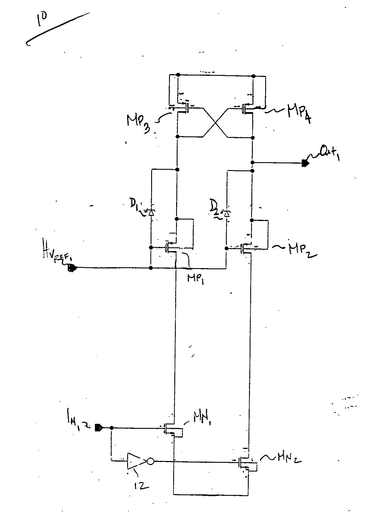
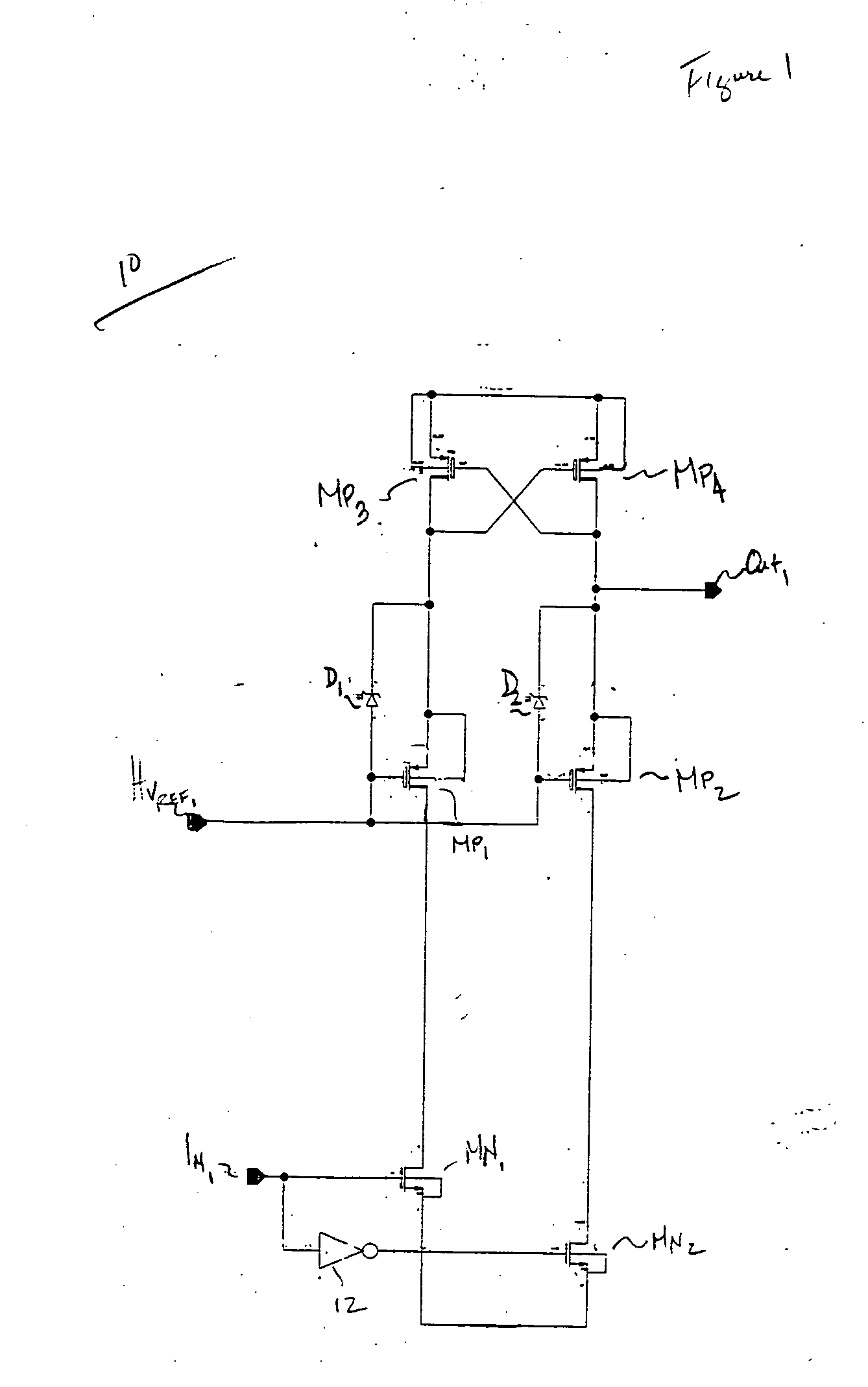
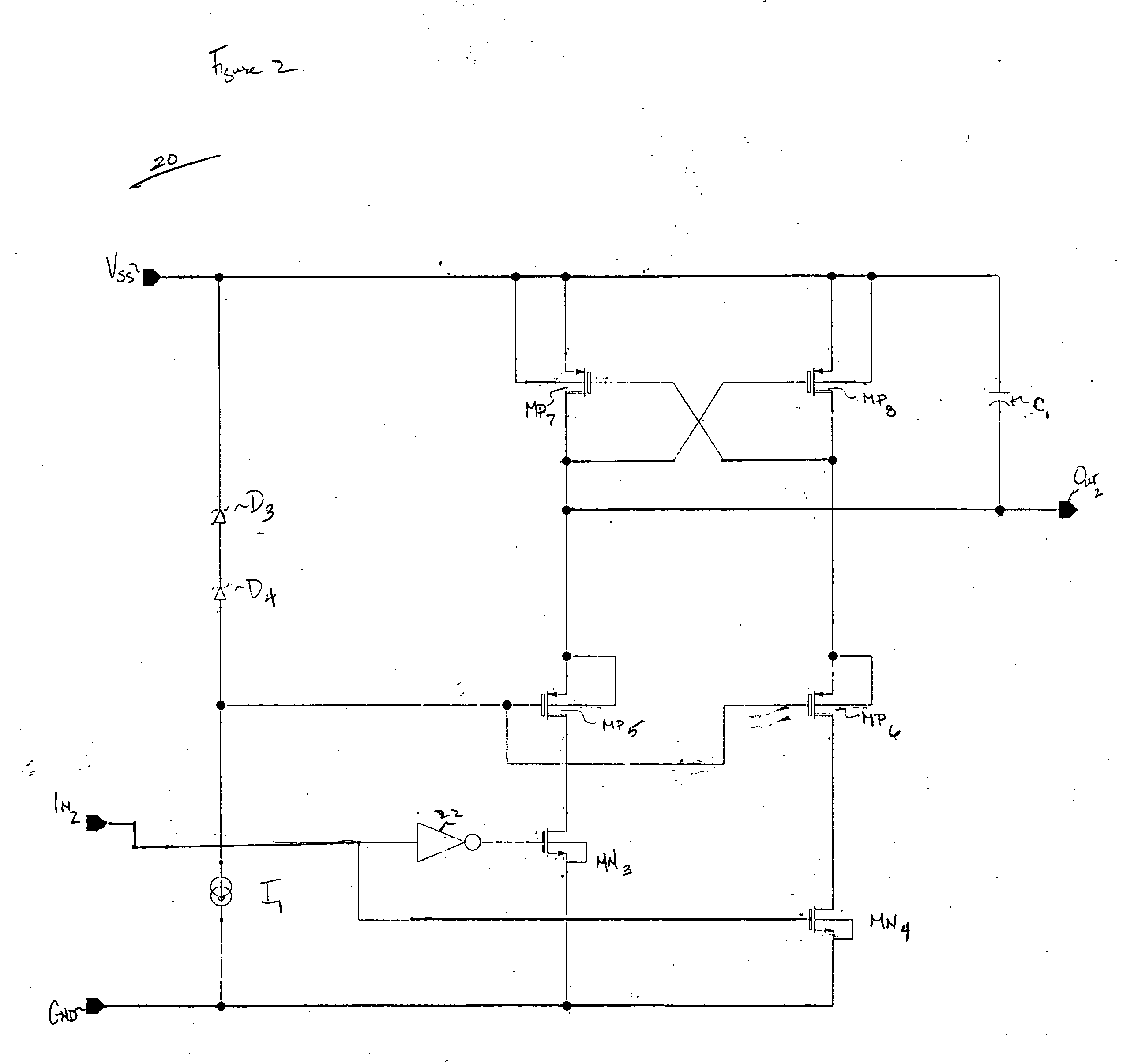
[0022] One or more exemplary implementations of the present invention will now be described with reference to the attached drawings, wherein like reference numerals are used to refer to like elements throughout. The various aspects of the invention are illustrated below in a high voltage level shifter, although the invention and the appended claims are not limited to the illustrated examples.

[0023] The present invention is best understood by comparison with the prior art. Hence, this detailed description begins with a discussion of known high voltage level shifter as is shown in FIG. 1. As shown, a low-voltage input signal IN1 is level-shifted to an high voltage output signal Out1. Transistors MN2 and MN1 are switched on and off, wherein when transistor MN2 is on, transistor MN1 is off. The converse is also true. In the instance, where input signal IN1 is a high signal, transistor MN1 will turn on. Current will flow through the drain node of transistor MN1 which pull down the gate ...


PUM


Abstract

A high voltage level shifter having a cost effective design that saves chip architecture and power. The high voltage level-shifter includes a resistor connected between a first node and a first power supply rail. An inverter couples to receive an input signal to provide an inverted input signal. A first circuit portion couples to receive the inverted input signal and connects between the first power supply rail and a second power supply rail for converting a high voltage signal into a low voltage signal. The first circuit portion includes a first clamp circuit, wherein the first circuit portion is biased through the first clamp circuit and the first node. A second circuit portion couples to receive the input signal and connects between the first power supply rail and a second power supply rail for converting a low voltage signal into a high voltage signal. The second circuit portion includes a second clamp circuit, wherein the second circuit portion is biased through the second clamp circuit and the first node. The second circuit portion provides a first internal bias for the first circuit portion and the first circuit portion provides a second internal bias for the second circuit portion. This high voltage level-shifter provides level shifting a low voltage signal (<5V) to a high voltage signal (˜40V), with no static power dissipation while still protecting all devices.

Description

FIELD OF THE INVENTION [0001] The present invention relates to level shifters and, more particularly, a self-biased high voltage level shifter. BACKGROUND OF THE INVENTION [0002] Many integrated circuits, such as display drivers, require a combination of high-voltage driving capability (an output voltage swing up to 100V or more) and a digital control using standard 5V CMOS logic. Hence, complex level-shifting circuits are needed to convert the 5V control signals into the desired high-voltage output waveforms. Moreover, in many of those applications, the system is battery-powered and very severe constraints are put on the power consumption of the level-shifters. One application where both high-voltage driving capability and low power consumption are required in the design of driver chips is in automotive applications. [0003] Level shifters, in general, are utilized in a circuit to transition from a low voltage signal to a high voltage signal. In the alternative, a level shifter may ...

Claims


Application Information

Patent Timeline
Patent Type & Authority Applications(United States)
IPC IPC(8): H03L5/00
CPCH03K3/356113H03K17/102
Inventor PAULETTI, TIMOTHY P.
Owner TEXAS INSTR INC
Why Eureka
Try Eureka