Method of forming ferroelectric thin film

a technology of ferroelectric thin film and a thin film layer, which is applied in the direction of natural mineral layered products, chemical coatings, liquid/solution decomposition chemical coatings, etc., can solve the problems of reducing the efficiency and reducing the cost of forming a thin film. , to achieve the effect of preventing material from easily volatilizing and minimizing the formation of oxygen vacancy

Inactive Publication Date: 2006-05-04
SAMSUNG ELECTRONICS CO LTD
View PDF5 Cites 3 Cited by
  • Summary
  • Abstract
  • Description
  • Claims
  • Application Information

AI Technical Summary

Benefits of technology

[0025] Further, in the method of the present invention, as the perovskite-type ferroelectric thin film is formed at a low temperature below the phase transition temperature, a thermal stress applied to the formed ferroelectric thin film may be minimized, and the formation of oxygen vacancy may be minimized. Furthermore, in the case that a material having a high volatility such as lead is involved, it may prevent the material from easily volatilization.

Problems solved by technology

Further, the selection of a substrate to be used is limited, and separation and crack of the layer during heating may occur [M. Yoshimura, S. E. Yoo, M. Hayashi and N. Ishizawa, “Preparation of BaTiO3 Thin Film by Hydrothermal electrochemical method”, Jpn. J. Appl. Phys., 28(11), L2007(1989)].
On account of this, in the device to require just a high dielectric constant of ferroelectric, or the device to require only spontaneous polarization of ferroelectric, the coexistence of the a-domain and c-domain may not be desirable (Ferroelectric Materials and Their Applications, Yuhuan Xu, 1991).
Further, in the ferroelectric thin film formed by the phase transition process, the holes formed inside the thin film due to poor layer coverage may cause an electric short phenomenon in upper and lower electrodes, and the analysis for electrical characteristics may be impossible.
As such, among the wet-type methods, the hydrothermal reaction process and the zol-gel method have many advantages, but the methods also have problems.

Method used


Image

  • Method of forming ferroelectric thin film
  • Method of forming ferroelectric thin film
  • Method of forming ferroelectric thin film

Examples


example

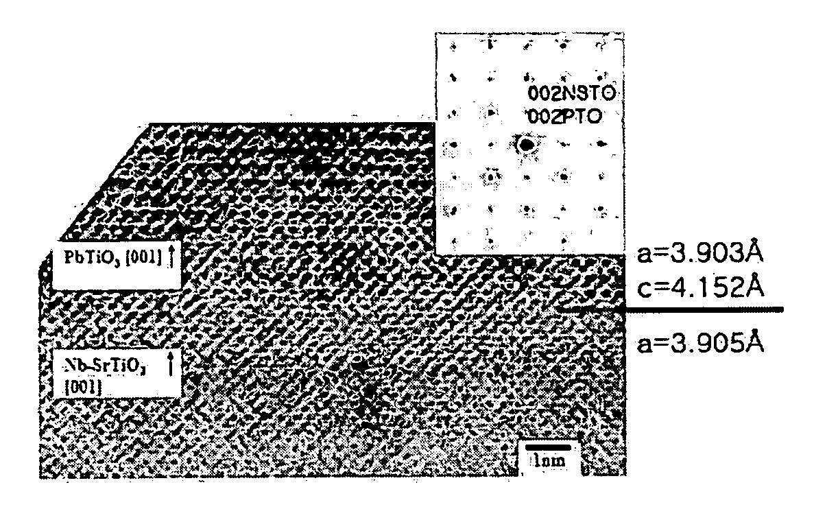
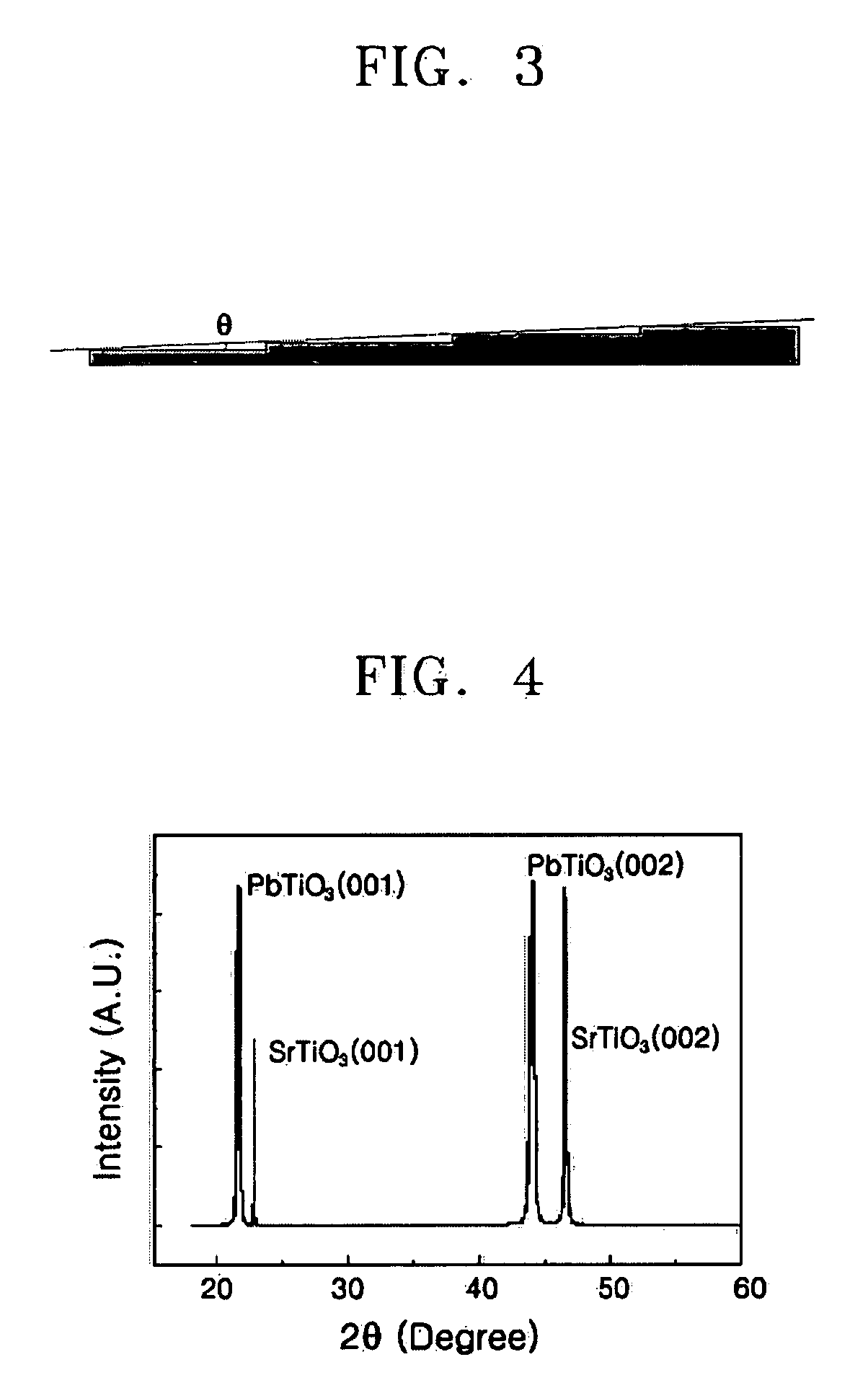
[0058] The substrate used in this example was composed of Nb—SrTiO3(001). The substrate had a miscut surface having an angle of 0.2°. The dimension of the substrate was 1 cm×1 cm×0.05 cm. A reaction solution for a hydrothermal reaction method was prepared by mixing 1 g of Pb(NO3)2, 0.2 g of TiO2 powder, and 20 ml of 8M KOH solution. The reaction solution and the Nb—SrTiO3 substrate were put into a high pressure reactor. The Nb—SrTiO3 substrate came to be immersed into the reaction solution inside the reactor. Then, a hydrothermal reaction process was performed on the reaction solution for 16 hours under the conditions of 200° C. of temperature and 15 MPa of pressure. By the process, a PbTiO3 thin film is formed on the miscut surface of the Nb—SrTiO3 substrate.

[0059] An XRD analysis result of the PbTiO3 thin film formed as above is shown in FIG. 4. In the XRD patterns of FIG. 4, a PbTiO3(001) peak and a PbTiO3(002) peak are shown high, while an SrTiO3(001) peak and an SrTiO3(002) pe...


PUM

PropertyMeasurementUnit
lattice constantaaaaaaaaaa
miscut angleaaaaaaaaaa

Abstract

A method of forming a ferroelectric thin film for suppressing the formation of a-domain and providing a sufficient layer coverage may be provided. The method includes immersing a substrate having the miscut surface into a reaction solution including a precursor compound for perovskite-type ferroelectric and water, and implementing a hydrothermal reaction in the reaction solution at a temperature lower than the phase transition temperature of the perovskite-type ferroelectric, thereby forming a perovskite-type ferroelectric thin film on the miscut surface of the substrate.

Description

BACKGROUND OF THE DISCLOSURE [0001] This application claims the priority of Korean Patent Application No. 10-2004-0088859, filed on Nov. 3, 2004, in the Korean Intellectual Property Office, the disclosure of which is incorporated herein in its entirety by reference. [0002] 1. Field of the Disclosure [0003] The disclosure relates to a method of forming a ferroelectric thin film, and particularly, to a method of forming a perovskite-type ferroelectric thin film. [0004] 2. Description of the Related Art [0005] Ferroelectrics mean a material having spontaneous polarization characteristics. In specific, after causing polarization in a ferroelectric material by an electric field, and then, even after removing the electric field, the ferroelectric material maintains the polarization state. As main examples of the ferroelectric having such a property, there are perovskite-type compounds, such as SrBi2Ta2O9(SBT) series, Pb(Zr, Ti)O3(PZT) series, or the like. Further, it is known that ferroel...

Claims


Application Information

Patent Timeline
Patent Type & Authority Applications(United States)
IPC IPC(8): B32B15/04B32B9/00B32B19/00
CPCC01G23/003C01P2002/72C01P2002/77C01P2004/03C01P2006/40C23C18/1216C23C18/1245H01L21/31691H01L21/02197H01L21/02282H01L21/31
Inventor PARK, JU-CHULCHOI, SI-KYUNGJUNG, WON-WOONG
Owner SAMSUNG ELECTRONICS CO LTD
Why Eureka
Try Eureka