Structures and methods for proximity communication using bridge chips

a technology of proximity communication and bridge chips, applied in the direction of semiconductor devices, semiconductor/solid-state device details, instruments, etc., can solve the problems of destroying received signals, not being able to align chips properly using existing mounting structures, and not being able to achieve the effect of properly aligning chips, simplifying system design, and reducing power consumption

a technology of proximity communication and bridge chips, applied in the direction of semiconductor devices, semiconductor/solid-state device details, instruments, etc., can solve the problems of destroying received signals, not being able to align chips properly using existing mounting structures, and not being able to achieve the effect of properly aligning chips, simplifying system design, and reducing power consumption

US20060095639A1Inactive Publication Date: 2006-05-04SUN MICROSYSTEMS INC

Image

  • Structures and methods for proximity communication using bridge chips
  • Structures and methods for proximity communication using bridge chips
  • Structures and methods for proximity communication using bridge chips

Examples


Embodiment Construction

[0054] The following description is presented to enable any person skilled in the art to make and use the invention, and is provided in the context of a particular application and its requirements. Various modifications to the disclosed embodiments will be readily apparent to those skilled in the art, and the general principles defined herein may be applied to other embodiments and applications without departing from the spirit and scope of the present invention. Thus, the present invention is not limited to the embodiments shown, but is to be accorded the widest scope consistent with the principles and features disclosed herein.

Challenges of Proximity Communication
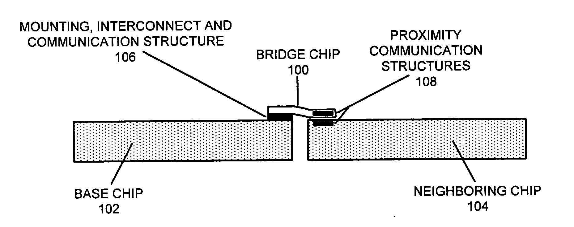
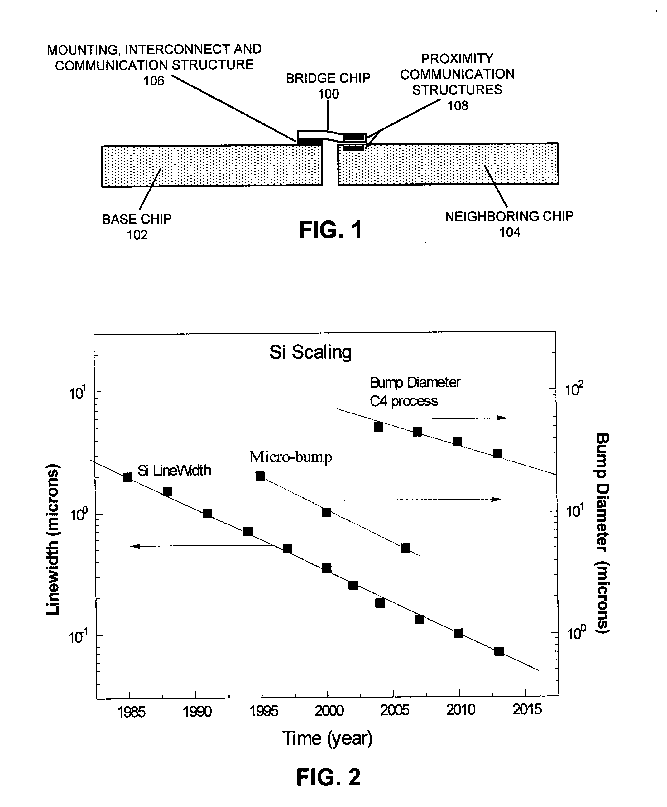
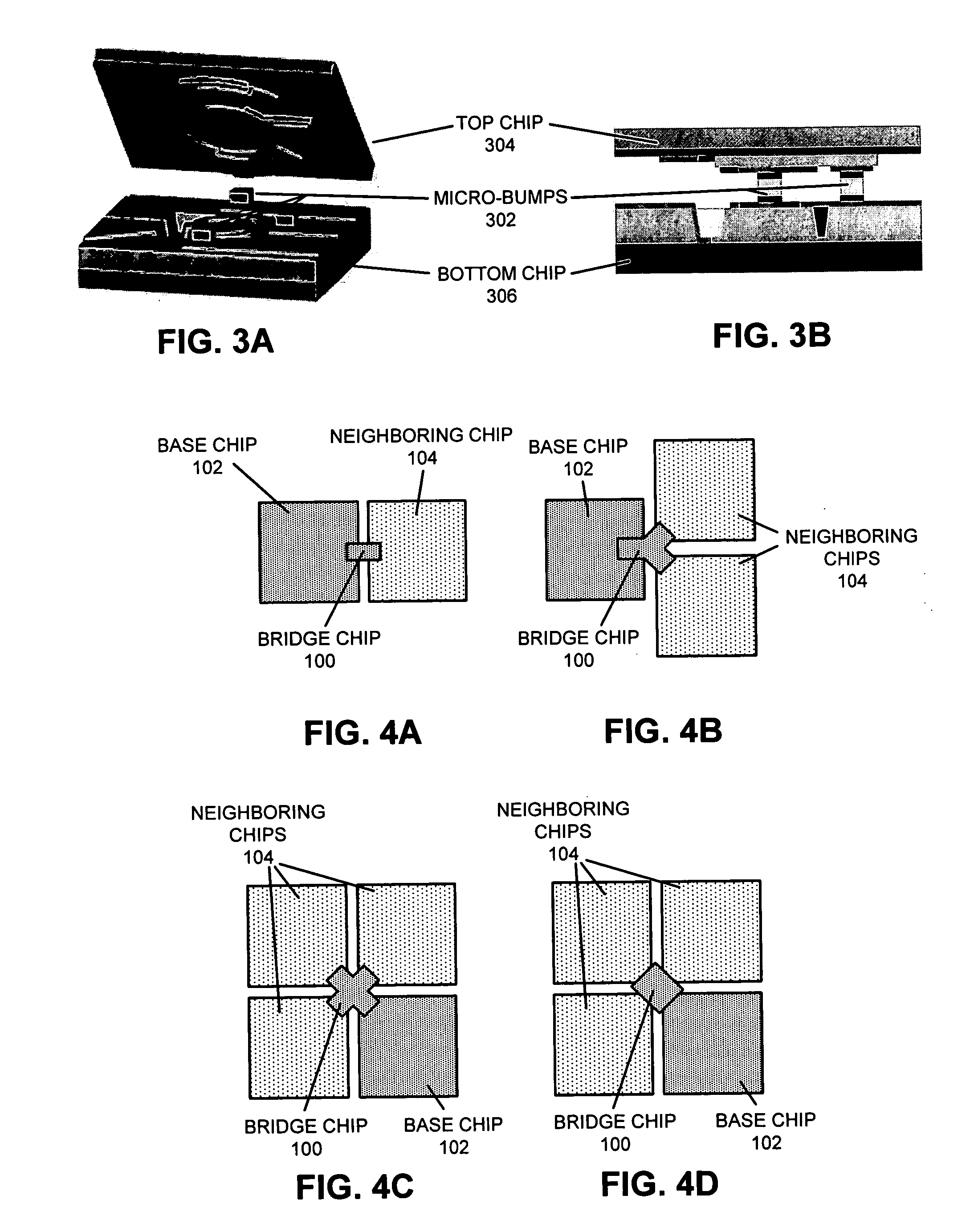
[0055]β€œProximity communication” makes possible direct chip-to-chip communication through capacitive coupling between mating arrays of pads on two closely-adjacent chips. Proximity communication enables extremely large bandwidth and bandwidth per area of an array, and enables large sets of densely-packed integrated circ...


PUM


Abstract

One embodiment of the present invention provides a system that facilitates proximity communication using a bridge chip. This system includes a base chip with an active face, upon which active circuitry and signal pads reside, and a back face opposite the active face. The bridge chip is mounted to the base chip using a mounting, interconnection, and communication structure. The bridge chip is positioned so that a free end is proximate to a neighboring chip, thereby supporting proximity communication between the base chip and the neighboring chip.

Description

RELATED APPLICATION [0001] This application claims priority under 35 U.S.C. 119(e) to U.S. Provisional Application Ser. No. 60 / 624,720, entitled β€œBridge Chip for Proximity Communication Between ICs in a Co-Planar Array,” by inventors Arthur R. Zingher, Bruce M. Guenin, Ronald Ho, Nyles I. Nettleton, Ashok V. Krishnamoorthy, and John E. Cunningham, filed on Nov. 2, 2004, the contents of which are herein incorporated by reference (Attorney Docket No. SUN05-0370PSP). GOVERNMENT LICENSE RIGHTS [0002] This invention was made with United States Government support under Contract No. NBCH020055 awarded by the Defense Advanced Research Projects Administration. The United States Government has certain rights in the invention.BACKGROUND [0003] 1. Field of the Invention [0004] The present invention generally relates to semiconductor integrated circuits. More specifically, the present invention relates to structures and methods for proximity communication using bridge chips. [0005] 2. Related Ar...

Claims


Application Information

Patent Timeline
04 May 2006
Publication
US20060095639A1
IPC
G06F13/36
CPC
H01L23/48; H01L25/0652; H01L25/0655; H01L2924/3011; H01L2924/0002; H01L2924/00
Inventors
GUENIN, BRUCE M.; ZINGHER, ARTHUR R.