

Semiconductor device
a technology of semiconductor modules and devices, applied in the field of semiconductor devices, can solve the problems of correspondingly increasing the size of devices as compared with semiconductor modules
- Summary
- Abstract
- Description
- Claims
- Application Information
AI Technical Summary
Benefits of technology
Problems solved by technology
Method used
Image

Examples
first embodiment
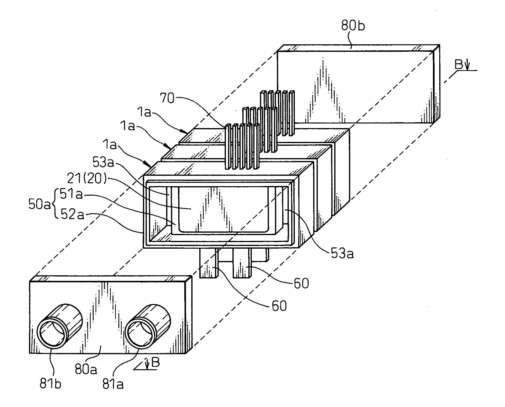
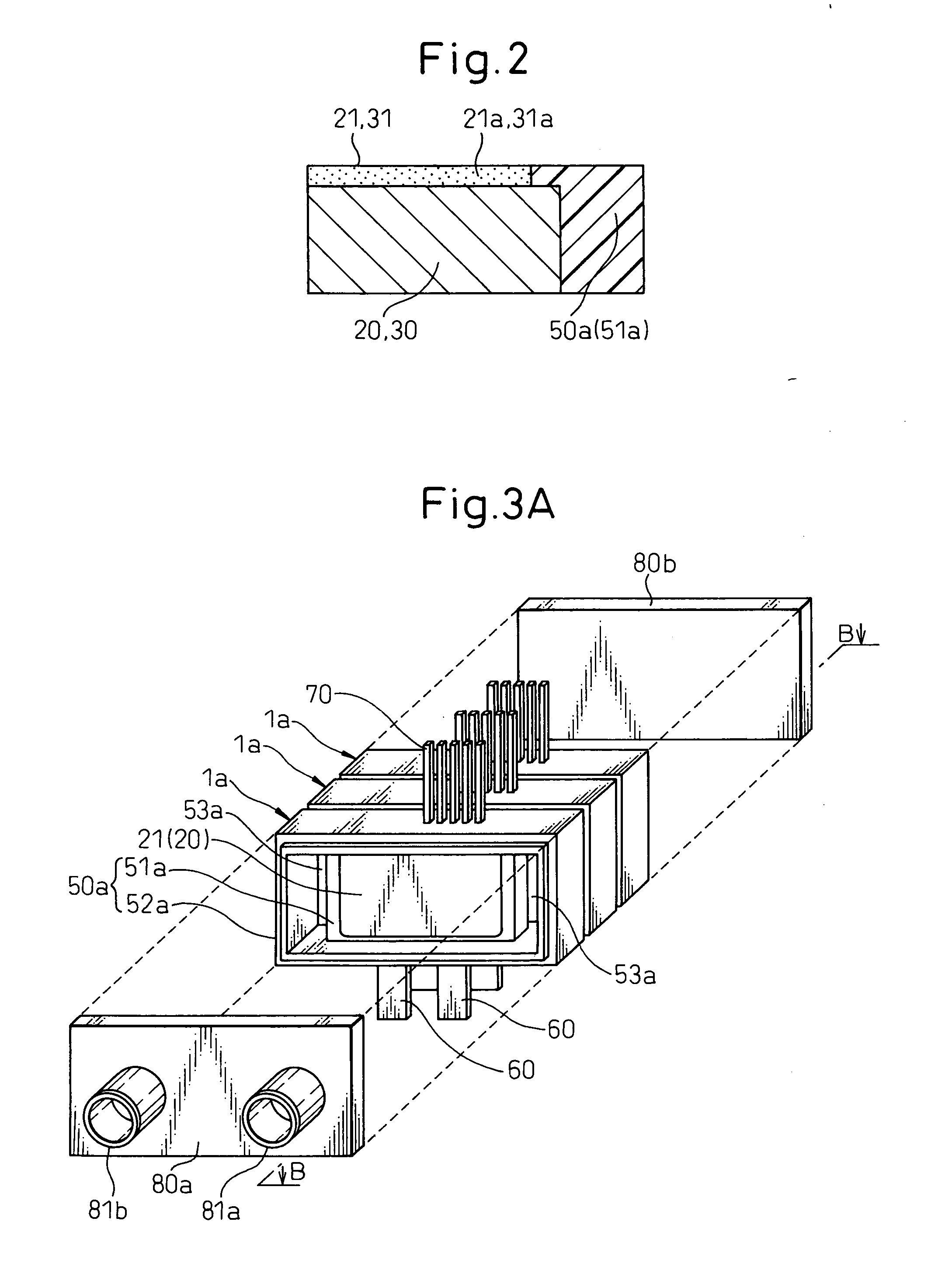
[0065]FIG. 1A is a perspective view showing a general configuration of a semiconductor device 100 according to a first embodiment of the invention. FIG. 1B is a diagram showing a sectional configuration along the one-dot chain line A-A in FIG. 1A.
[0066] As shown in FIGS. 1A, 1B, the semiconductor device 100 according to this embodiment is mainly configured of a semiconductor module 1a.
[0067] The semiconductor module 1 shown in FIGS. 1A, 1B includes a first semiconductor chip 11 and a second semiconductor chip 12 as semiconductor elements, a lower heat sink 20 as a first metal plate, an upper heat sink 30 as a second metal plate, solder 41, 42 as conductive joint interposed between the semiconductor elements and the lower heat sink 20 or the upper heat sink 30, and a molded resin 50 as a seal member.
[0068] In the semiconductor module 1a according to this embodiment, as shown in FIGS. 1A and 1B, the first semiconductor chip 11 and the second semiconductor chip 12 are arranged in pa...
second embodiment
[0140] According to the second embodiment of the invention, the heat radiation surfaces 21, 31 of the heat sinks 20, 30 are formed with fins or the like to improve the heat radiation performance.
[0141]FIG. 4 is a perspective view schematically showing a configuration of a semiconductor device 200 according to the second embodiment of the invention. FIG. 5A is a diagram showing an example of the sectional configuration along a one-dot chain line C-C in FIG. 4, and FIG. 5B a diagram showing another example of the sectional configuration along a one-dot chain line C-C in FIG. 4.
[0142] In the semiconductor device according to the first embodiment, heat is radiated from the heat radiation surfaces 21, 31 of the heat sinks 20, 30 made of metal. To improve the heat radiation performance, therefore, the heat radiation surfaces 21, 31 preferably have rough surfaces.
[0143] The rough heat radiation surfaces 21, 31 are formed by being roughened or grooved by etching or machining.
[0144] Also...
third embodiment
[0161] According to the third embodiment of the invention, a position of the openings formed as a refrigerant path in the molded resin is different from that of the opening in the first and second embodiments. FIGS. 6A, 6B are schematic diagrams showing a semiconductor device 300 according to the third embodiment of the invention. FIG. 6A is a perspective view, and FIG. 6B a side view as taken in the direction of arrow A′.
[0162] In the first and second embodiments, the refrigerant path 53 is formed as openings 53 between the sealing part 51 and the wall part 52 of the molded resin 50.
[0163] In the semiconductor device 300 according to this embodiment, in contrast, as shown in FIGS. 6A, 6B, the molded resin 50b includes the sealing part 51b and the wall part 52b, and the refrigerant path is formed as the openings 53b on the wall part 52b. This openings 53b is indicated as an area hatched for convenience sake in FIG. 6B.
[0164] Also according to this embodiment, the semiconductor de...
PUM
 Abstract
Description
Claims
Application Information