Semiconductor light-emitting device, method for fabricating the same, lighting module and lighting apparatus having semiconductor light-emitting device

a semiconductor and light-emitting device technology, applied in the direction of semiconductor devices for light sources, lighting and heating apparatus, solid-state devices, etc., can solve the problems of thermal saturation of light output, poor heat dispersion, and the light-emitting device using the first feeding method cannot achieve sufficient heat dispersion, so as to enhance the yield of semiconductor light-emitting devices, and prevent cracking or chipping

Active Publication Date: 2006-05-11
PANASONIC SEMICON SOLUTIONS CO LTD
View PDF6 Cites 43 Cited by
  • Summary
  • Abstract
  • Description
  • Claims
  • Application Information

AI Technical Summary

Benefits of technology

[0097] As mentioned above, in the semiconductor light-emitting device according to the present invention, the semiconductor light-emitting element is fed with power through the wiring metal, not a bonding wire. With this structure, the semiconductor light-emitting device can be fabricated without applying pressure to the semiconductor light-emitting element. This makes it possible to prevent cracking or chipping from occurring in the semiconductor light-emitting element by giving pressure to the semiconductor light-emitting element during manufacturing. As a result, the yield of semiconductor light-emitting devices can be enhanced.
[0098] In particular, in the case of the semiconductor light-emitting device in which the plurality of semiconductor light-emitting elements are arranged in an array, each of the semiconductor light-emitting elements is fed with power through not the bonding wire but the common wiring metal. Therefore, the yield of semiconductor light-emitting devices can be further enhanced.
[0099] Moreover, since there is no need to form a pad electrode on a light extraction surface of the semiconductor light-emitting element, the area of the effective light extraction surface of the semiconductor light-emitting element can be increased and, therefore, the light emission efficiency can be enhanced.

Problems solved by technology

The sapphire substrate has large thermal resistance and thus poor heat dispersion.
Therefore, the semiconductor light-emitting device using the first feeding method cannot achieve sufficient heat dispersion.
As a result, when the semiconductor light-emitting device is applied to illumination or the like that requires a large mount of power, problems such as thermal saturation of light output and decrease of reliability of light output arise.
In addition, in the semiconductor light-emitting device using the second feeding method, only Au bumps serve as paths for heat dispersion and, therefore, sufficient heat dispersion cannot be achieved.
As a result, also when the semiconductor light-emitting device is applied to illumination or the like that requires a large amount of power, problems such as thermal saturation of light output and decrease of reliability of light output arise.
However, the results of the inventors' experiments on the conventional semiconductor light-emitting device using laser lift-off technique have shown the following problems.
Therefore, during wire bonding, the semiconductor light-emitting element is deformed by application of ultrasound or local application of pressure from the tip part of a collet for wire bonding, and thereby causes cracking or chipping.
As a result, there found a problem of significantly reducing yield of the semiconductor light-emitting device.
As a result, there found a problem of generating cracking or chipping in the semiconductor light-emitting element.
Therefore, there found a problem that the larger the number of semiconductor light-emitting elements arranged in an array is, the significantly lower the yield of semiconductor light-emitting devices is.
As a result, there found a problem that sufficient light emission efficiency cannot be obtained.

Method used


Image

  • Semiconductor light-emitting device, method for fabricating the same, lighting module and lighting apparatus having semiconductor light-emitting device
  • Semiconductor light-emitting device, method for fabricating the same, lighting module and lighting apparatus having semiconductor light-emitting device
  • Semiconductor light-emitting device, method for fabricating the same, lighting module and lighting apparatus having semiconductor light-emitting device

Examples


first embodiment

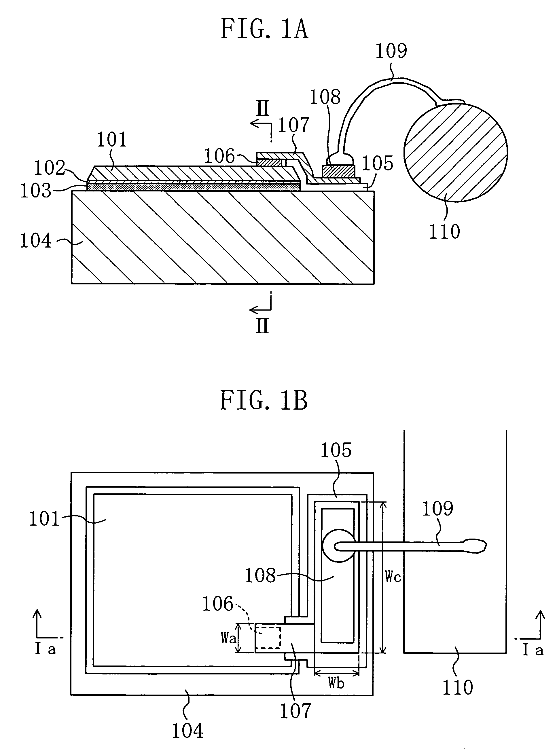
[0116] First, referring to FIGS. 1A and 1B, the structure of a semiconductor light-emitting device according to a first embodiment of the present invention will be described.

[0117]FIGS. 1A and 1B are diagrams showing the structure of the semiconductor light-emitting device according to the first embodiment of the present invention. Note that FIG. 1A is a cross sectional view showing the structure of the semiconductor light-emitting device according to the first embodiment of the present invention, specifically, a cross sectional view taken along line Ia-Ia of FIG. 1B and FIG. 1B is a plan view showing the same.

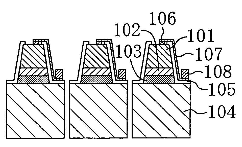
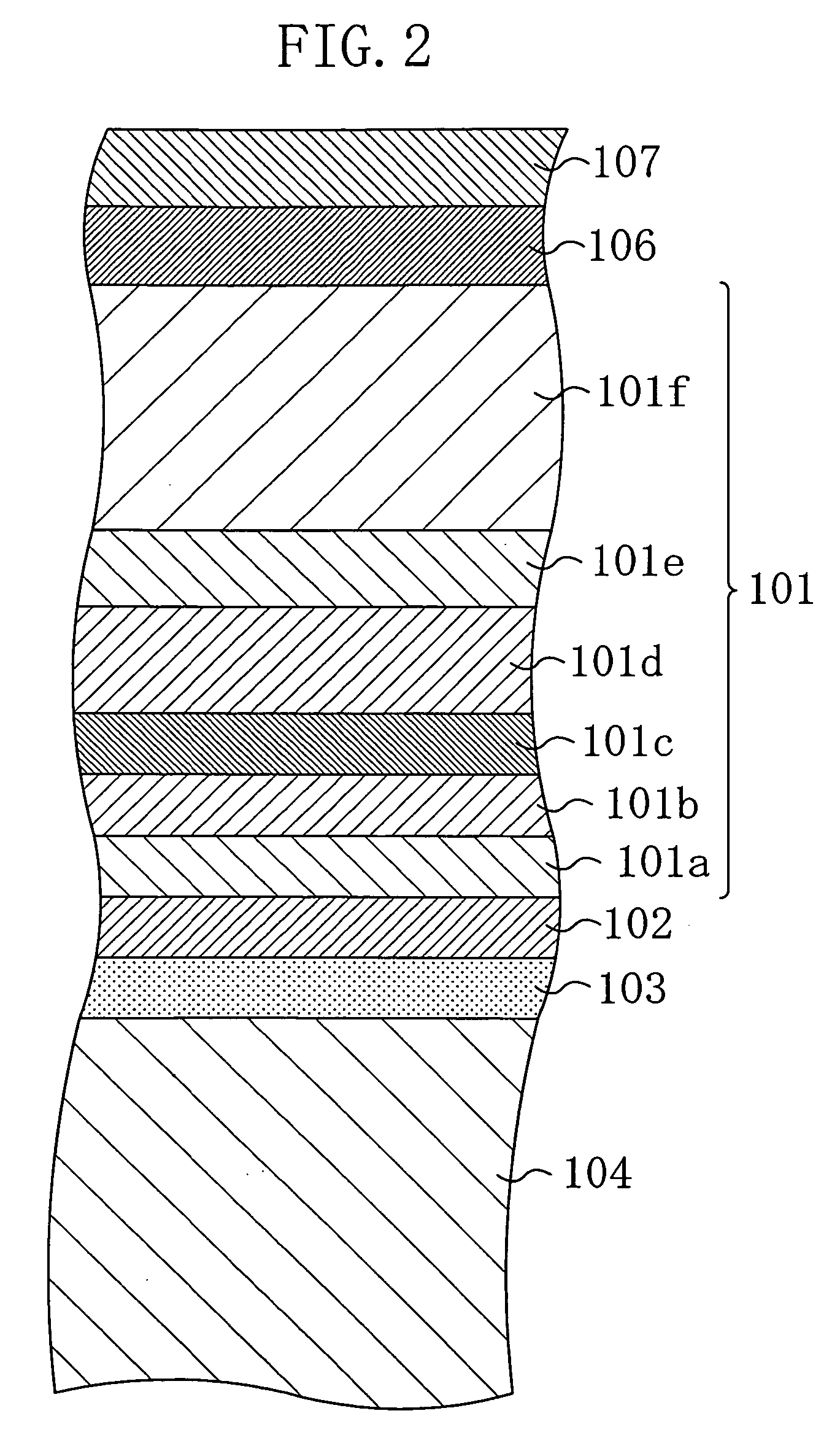
[0118] As illustrated in FIG. 1A, a p-side ohmic electrode 102, a pn junction structure 101, and an n-side ohmic electrode 106 are sequentially formed on a support 104 made of CuW with a fusion material 103 interposed between the support 104 and the p-side ohmic electrode 102. The pn junction structure 101 has a thickness of 5 μm and a 350 μm square shape, and comprises a se...

second embodiment

[0177] Now, referring to FIGS. 6A and 6B, the structure of a semiconductor light-emitting device according to a second embodiment of the present invention will be described.

[0178]FIGS. 6A and 6B are diagrams showing the structure of the semiconductor light-emitting device according to the second embodiment of the present invention. FIG. 6A is a cross sectional view showing the structure of the semiconductor light-emitting device according to the second embodiment of the present invention, specifically, a cross sectional view taken along line VIa-VIa of FIG. 6B and FIG. 6B is a plan view showing the same.

[0179] As illustrated in FIG. 6A, a p-side ohmic electrode 202, a pn junction structure 201, and an n-side ohmic electrode 205 are sequentially formed on a support 203 which has a thickness of 100 μm and is made of Au. The pn junction structure 201 has a thickness of 5 μm and a 350 μm square shape, and comprises a semiconductor layer formed by sequentially depositing a p-type galli...

third embodiment

[0227] Now, referring to FIG. 9, the structure of a semiconductor light-emitting device according to a third embodiment of the present invention will be described.

[0228]FIG. 9 is a plan view of the structure of the semiconductor light-emitting device according to the third embodiment of the present invention.

[0229] As being identical with the cross sectional view of the structure of the semiconductor light-emitting device according to the first embodiment, the cross sectional view of the structure of the semiconductor light-emitting device according to the third embodiment of the present invention is omitted here. In FIG. 9, the same structural elements as in the semiconductor light-emitting device according to the first embodiment of the present invention are denoted by the same reference numerals. In the third embodiment, the same description as in the semiconductor light-emitting device according to the first embodiment of the present invention will not be repeated.

[0230] As i...


PUM


Abstract

A semiconductor light-emitting device includes: a support; a semiconductor light-emitting element bonded to the support and comprising a first electrode, a second electrode, and a semiconductor layer including at least an active layer, at least one of the first and second electrodes overlying the semiconductor layer; and a wiring metal formed to extend from above a portion of an upper surface of the support not underlying the semiconductor light-emitting element to one said electrode overlying the semiconductor layer. The electrode is fed with power through the wiring metal.

Description

CROSS-REFERENCE TO RELATED APPLICATIONS [0001] The present application claims priority under 35 USC 119(a) to Japanese Patent Application No. 2004-328182 filed on Nov. 11, 2004, the entire contents of which are hereby incorporated by reference. BACKGROUND OF THE INVENTION [0002] (a) Field of the Invention [0003] The present invention relates to a semiconductor light-emitting device having a light-emitting diode or the like, and particularly to a semiconductor light-emitting device used for lighting modules or lighting apparatuses, and a method for fabricating the same. [0004] (b) Description of Related Art [0005] Recently, as the luminance of a white light-emitting diode (hereinafter referred to as “LED”) increases, the application of LEDs is greatly expanded from for indication to for illumination. [0006] In general, the white LED has a structure in which a semiconductor light-emitting element for emitting blue or ultraviolet light in combined with a phosphor that is excited by the...

Claims


Application Information

Patent Timeline
Patent Type & Authority Applications(United States)
IPC IPC(8): H01L33/00H01L33/06H01L33/08H01L33/32H01L33/36H01L33/44H01L33/50H01L33/62
CPCF21K9/00H01L33/385H01L33/62H01L2224/45144H01L2924/00014H01L24/48H01L2224/48465H01L2224/48091H01L2924/01029H01L24/45H01L2924/12036H01L2924/12041H01L2224/05599H01L2924/00
Inventor YURI, MASAAKI
Owner PANASONIC SEMICON SOLUTIONS CO LTD
Why Eureka
Try Eureka