Cross-point nonvolatile memory devices using binary metal oxide layer as data storage material layer and methods of fabricating the same

a non-volatile memory and data storage technology, applied in the direction of digital storage, semiconductor/solid-state device details, digital storage, etc., can solve the problems of difficult to pattern the pcmo layer or the htsc material layer, and the composition ratio of the material layer may not be uniform across the device,

Active Publication Date: 2006-05-11
SAMSUNG ELECTRONICS CO LTD
View PDF11 Cites 81 Cited by
  • Summary
  • Abstract
  • Description
  • Claims
  • Application Information

AI Technical Summary

Benefits of technology

[0044] As described above, embodiments of the present invention can provide cross-point nonvolatile memory devices using a binary metal oxide layer as a data storage material layer. According to exemplary embodiments of the present invention, highly integrated resistance RAM devices, which can stably operate at low voltage, may be provided.
[0045] Also, diodes are formed in respective cells of the resistance RAM devices, which can reduce crosstalk between adjacent cells caused by a leakage current and can also reduce power consumption.

Problems solved by technology

Accordingly, the composition ratio of the material layer may be non-uniform across the device.
Also, it may be difficult to pattern the PCMO layer or the HTSC material layer using typical photolithography and etching processes, which are widely used in the fabrication of semiconductor devices.
However, since the above-described noble metals are chemically very stable, they may be difficult to polish by the CMP process to form the lower electrode.

Method used


Image

  • Cross-point nonvolatile memory devices using binary metal oxide layer as data storage material layer and methods of fabricating the same
  • Cross-point nonvolatile memory devices using binary metal oxide layer as data storage material layer and methods of fabricating the same
  • Cross-point nonvolatile memory devices using binary metal oxide layer as data storage material layer and methods of fabricating the same

Examples


Embodiment Construction

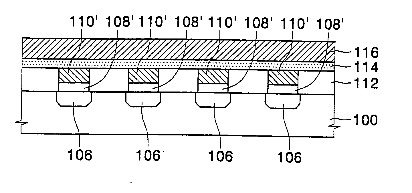
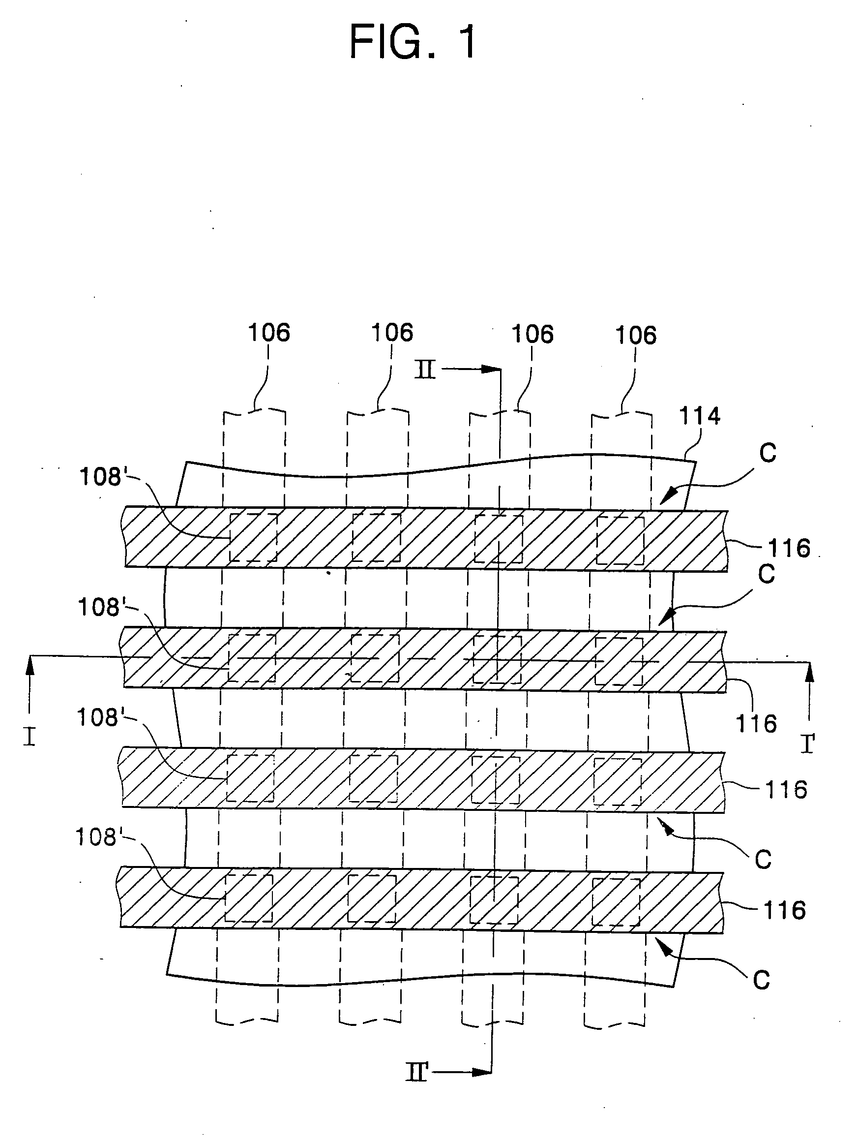
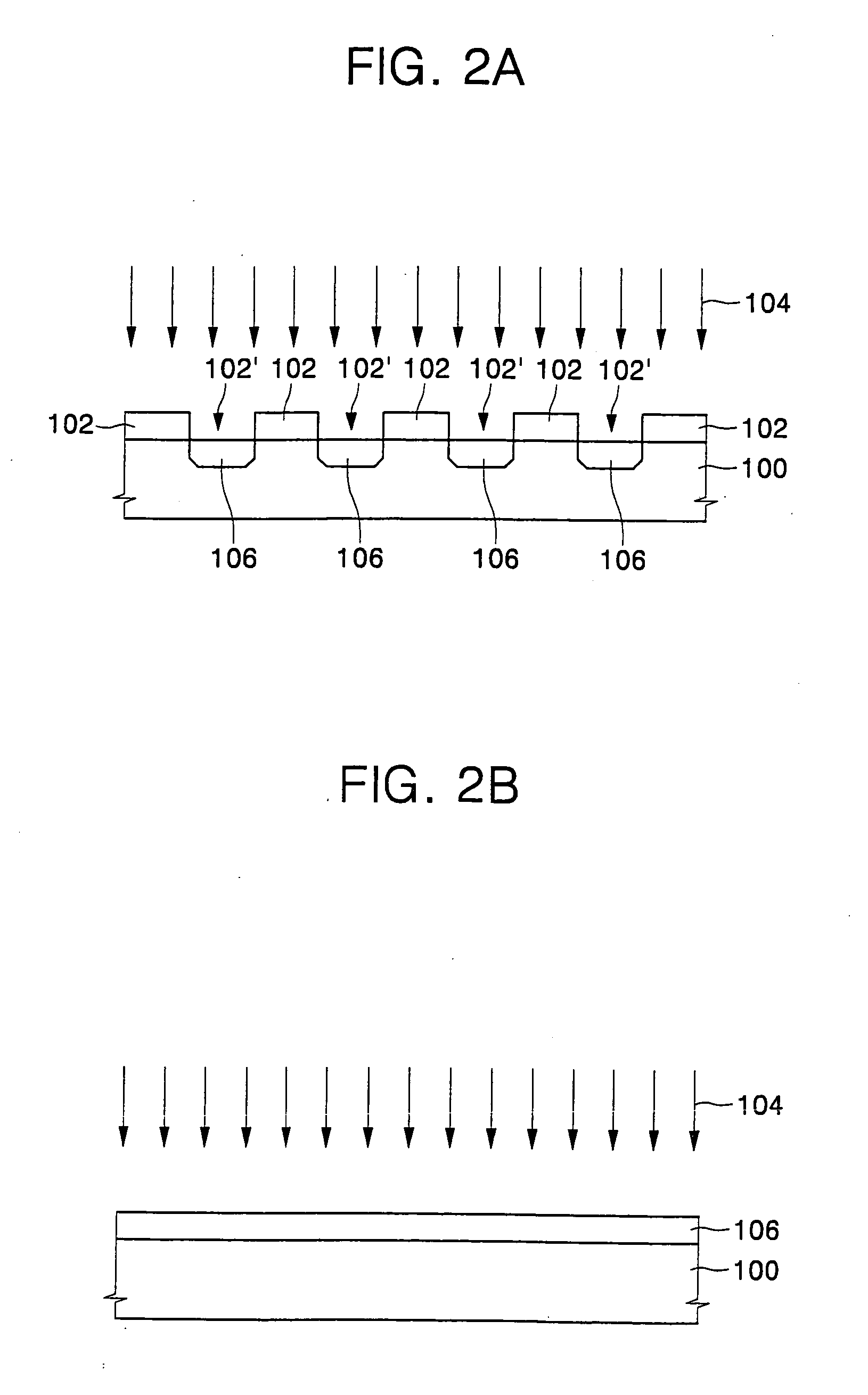
[0024] The invention now will be described more fully hereinafter with reference to the accompanying drawings, in which embodiments of the invention are shown. This invention may, however, be embodied in many different forms and should not be construed as limited to the embodiments set forth herein. Rather, these embodiments are provided so that this disclosure will be thorough and complete, and will fully convey the scope of the invention to those skilled in the art. Moreover, each embodiment described and illustrated herein includes its complementary conductivity type embodiment as well. Like numbers refer to like elements throughout.

[0025] It will be understood that when an element is referred to as being “connected”, “responsive” or “in response to” another element, it can be directly connected, responsive or in response to the other element or intervening elements may be present. In contrast, the term “directly” means there are no intervening elements present. As used herein, ...


PUM

PropertyMeasurementUnit
angleaaaaaaaaaa
voltageaaaaaaaaaa
conductivityaaaaaaaaaa

Abstract

A cross-point nonvolatile memory device using a binary metal oxide layer as a data storage material layer includes spaced apart doped lines disposed in a substrate. Spaced apart upper electrodes cross over the doped lines such that cross points are formed where the upper electrodes overlap the doped lines. Lower electrodes are disposed at the cross points between the doped lines and the upper electrodes. A binary metal oxide layer is provided between the upper electrodes and the lower electrodes and provided as a data storage material layer. Doped regions are provided between the lower electrodes and the doped lines and form diodes together with the doped lines. The doped regions have an opposite polarity to the doped lines

Description

CROSS-REFERENCE TO RELATED APPLICATION [0001] This application claims the benefit under 35 USC § 119 of Korean Patent Application No. 10-2004-0091554 filed on Nov. 10, 2004, the disclosure of which is hereby incorporated herein by reference in its entirety as if set forth fully herein. FIELD OF THE INVENTION [0002] The present invention relates to nonvolatile memory devices and methods of fabricating the same and, more particularly, to cross-point nonvolatile memory devices and methods of fabricating the same. BACKGROUND OF THE INVENTION [0003] Nonvolatile memory devices do not lose data stored therein even if power is interrupted. Thus, nonvolatile memory devices are being widely employed in computers, mobile communication terminals, memory cards, and the like. [0004] A flash memory device is commonly used as a nonvolatile memory device. In general, the flash memory device includes memory cells, each of which has a stacked gate structure. The stacked gate structure may include a tu...

Claims


Application Information

Patent Timeline
Patent Type & Authority Applications(United States)
IPC IPC(8): H01L21/82H01L27/10G11C13/00H01L27/24H01L45/00
CPCG11C13/0007G11C2213/32H01L45/04H01L45/1233H01L45/146H01L27/2409H01L27/2472H10B63/20H10B63/82H10N70/20H10N70/826H10N70/8833
Inventor BAEK, IN-GYULEE, MOON-SOOK
Owner SAMSUNG ELECTRONICS CO LTD
Why Eureka
Try Eureka