Nano-VCSEL device and fabrication thereof using nano-colonnades

a nano-colonnade and laser technology, applied in the field of nano-scale laser devices and their fabrication, can solve the problems of inability to reproduce, inconvenient, expensive and sometimes tedious interconnection techniques of nanowires with other circuit elements, and inability to make contact with surfaces, etc., to achieve reproducible mass-fabrication of nano-scale devices such as dense, low-cost device arrays, and avoid the effect of aging

Active Publication Date: 2006-05-11
SAMSUNG ELECTRONICS CO LTD
View PDF14 Cites 58 Cited by
  • Summary
  • Abstract
  • Description
  • Claims
  • Application Information

AI Technical Summary

Problems solved by technology

However, available techniques for interconnection of the nanowires with other circuit elements, such as between electrodes of a nano-scale device, tend to be tedious, expensive and sometimes not reproducible.
As such, these techniques are limited to making contact to surfaces usually one nanowire (or one nanowire end) at a time.
While these techniques are useful in a research environment and facilitate characterization studies using nanowires, they are not conducive to, and not suitable for, reproducible mass-fabrication of nano-scale devices, such as dense, low-cost device arrays, in a manufacturing environment.

Method used


Image

  • Nano-VCSEL device and fabrication thereof using nano-colonnades
  • Nano-VCSEL device and fabrication thereof using nano-colonnades
  • Nano-VCSEL device and fabrication thereof using nano-colonnades

Examples


Embodiment Construction

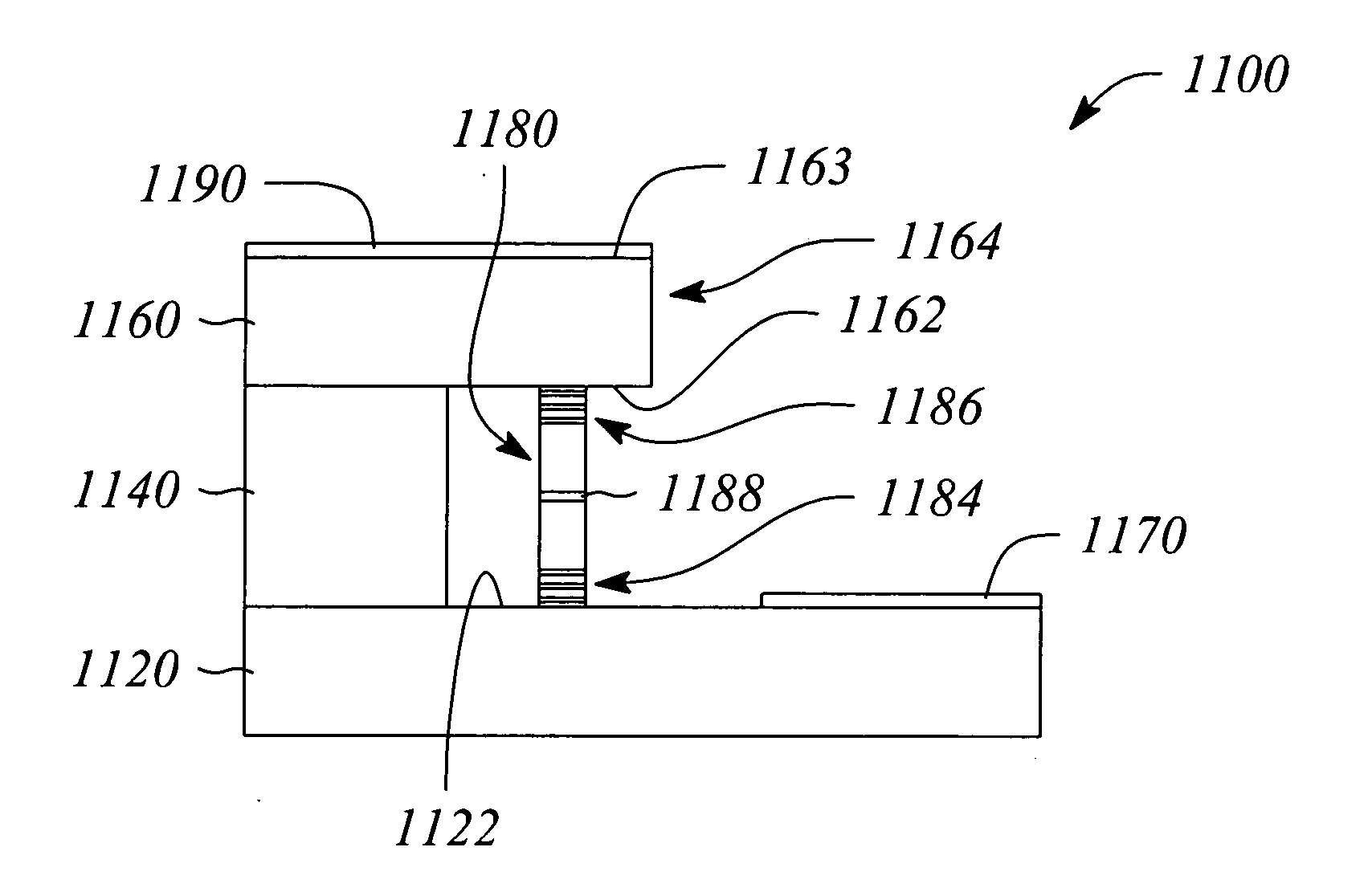
[0021] Embodiments of the present invention are directed to a nanowire grown to interconnect vertically spaced apart horizontal surfaces. The horizontal surface from which the nanowire grows is a (111) surface of a [111] oriented semiconductor crystal lattice. A semiconductor nanowire will grow preferentially nearly normal to the (111) surface. On a horizontally oriented (111) surface, the nanowire will grow from the (111) surface, as a column. The nanowire column growth may be akin to stalagmite growth in geology, for example and not by way of limitation. The nanowire column will grow nearly or substantially vertically at least until it contacts a facing horizontal surface. By ‘nearly vertically’ or ‘substantially vertically’ it is meant that the nanowire will grow from the (111) horizontal surface predominantly in a direction to connect to the facing horizontal surface. Once contacted, the nanowire column will attach or connect to the facing horizontal surface. The crystal orienta...


PUM


Abstract

A nano-colonnade VCSEL device and a method of fabrication utilize a nanowire column grown nearly vertically from a (111) horizontal surface of a first layer to another horizontal surface of a second layer to connect the layers. The VCSEL device includes a first layer having the (111) horizontal surface; a second layer; and an insulator support between the first layer and the second layer that separates the first layer from the second layer. A portion of the second layer overhangs the insulator support, such that a horizontal surface of the overhanging portion is spaced from and faces the (111) horizontal surface of the first layer. The VCSEL device further includes a nanowire column extending nearly vertically from the (111) horizontal surface to the facing horizontal surface, and distributed Bragg mirrors adjacent to opposite end of the nanowire column.

Description

CROSS-REFERENCE TO RELATED APPLICATIONS [0001] This application is a continuation in part (CIP) of co-pending patent application of M. Saif Islam et al., Ser. No. 10 / 982,051, filed Nov. 5, 2004.BACKGROUND [0002] 1. Technical Field [0003] The invention relates to nanotechnology. In particular, the invention relates to nano-scale laser devices and their fabrication. [0004] 2. Description of Related Art [0005] A consistent trend in semiconductor technology since its inception is toward smaller and smaller device dimensions and higher and higher device densities. As a result, an area of semiconductor technology that recently has seen explosive growth and generated considerable interest is nanotechnology. Nanotechnology is concerned with the fabrication and application of so-called nano-scale structures, structures having at least one linear dimension between 1 nm and 200 nm. These nano-scale structures are often 50 to 100 times smaller than conventional semiconductor structures. [0006] ...

Claims


Application Information

Patent Timeline
Patent Type & Authority Applications(United States)
IPC IPC(8): H01S5/00
CPCB82Y10/00B82Y20/00H01L29/0665H01L29/0673H01L29/0676H01L29/068Y10S977/951H01S5/041H01S5/183H01S5/341H01S5/3412H01S5/3428H01S5/0261H01S5/026H01S5/18341H01S5/423
Inventor WANG, SHIH-YUANISLAM, M. SAIF
Owner SAMSUNG ELECTRONICS CO LTD
Why Eureka
Try Eureka