Method for detection and relocation of wafer defects

a technology of defect detection and defect relocation, applied in the direction of individual semiconductor device testing, semiconductor/solid-state device testing/measurement, instruments, etc., can solve the problems of defect often occurring, missing or extra patterns, and extraneous material that gets deposited on the wafer surface, etc., and achieves the effect of easy placement in the sem

a technology of defect detection and defect relocation, applied in the direction of individual semiconductor device testing, semiconductor/solid-state device testing/measurement, instruments, etc., can solve the problems of defect often occurring, missing or extra patterns, and extraneous material that gets deposited on the wafer surface, etc., and achieves the effect of easy placement in the sem

US20060100730A1Inactive Publication Date: 2006-05-11JEOL USA

Image

  • Method for detection and relocation of wafer defects
  • Method for detection and relocation of wafer defects
  • Method for detection and relocation of wafer defects

Examples


Embodiment Construction

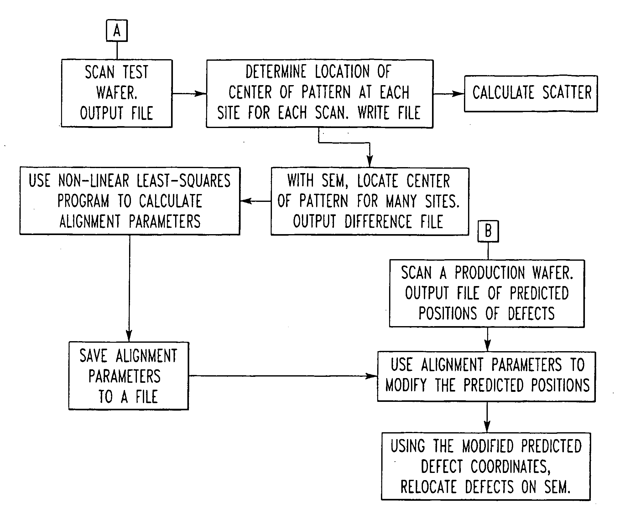
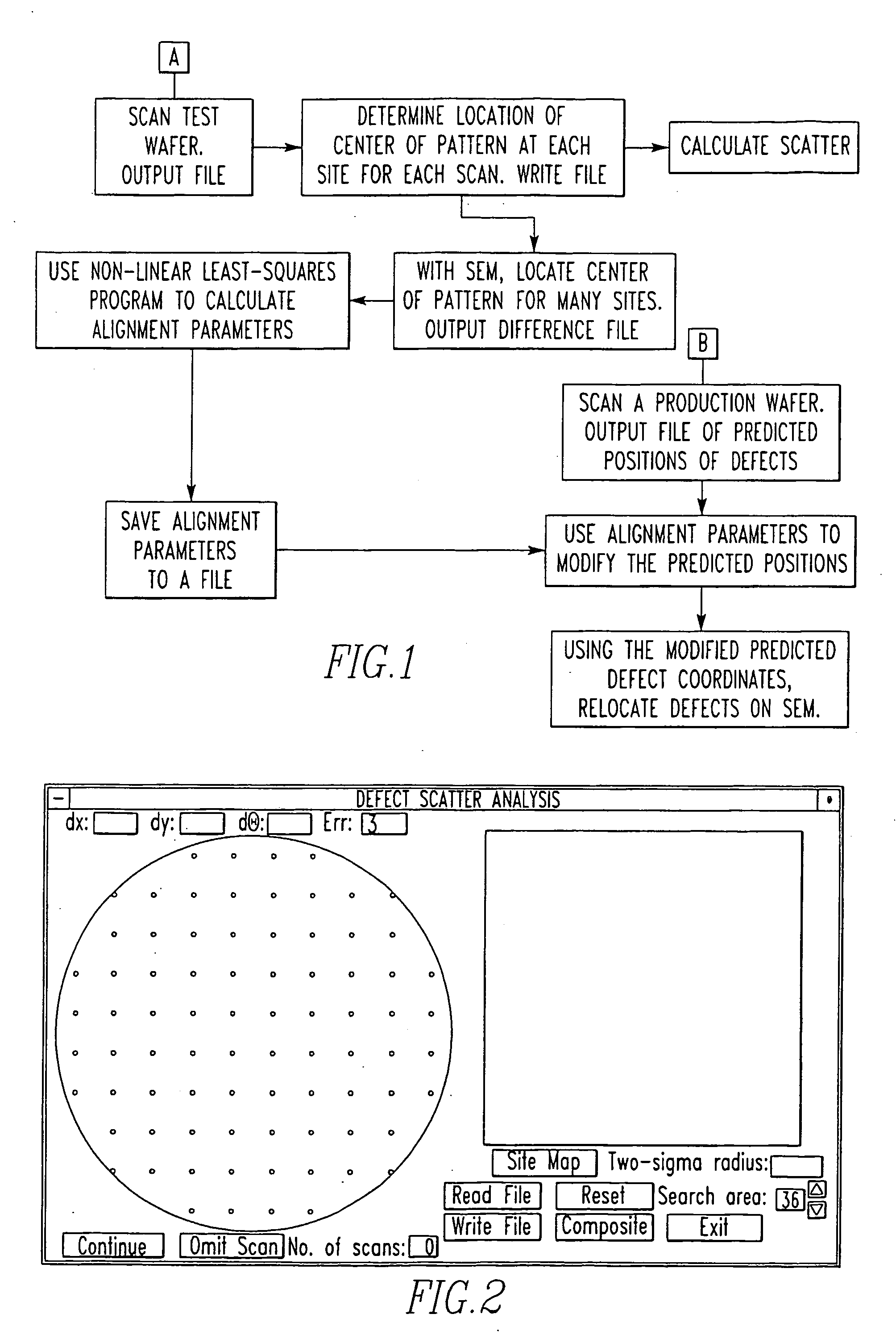
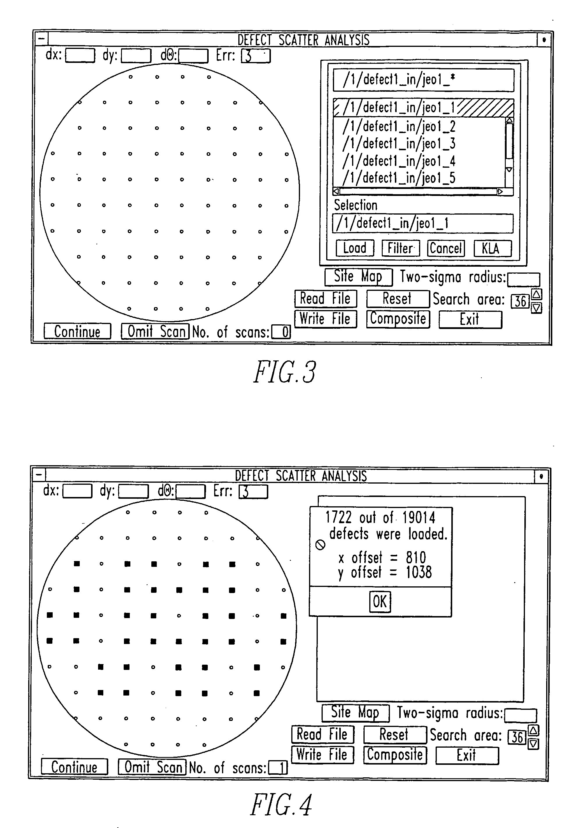
[0030] Referring now to FIG. 1, the method according to the present invention involves five basic steps: 1) A special test wafer with a pattern of markers repeated at many sites is scanned multiple times with a defect scanner. For each scan, the wafer is loaded, aligned, scanned, and unloaded and a defect file containing the coordinates of all defects detected during the scan is saved; 2) Each file is analyzed, using pattern recognition techniques to locate the center point of the pattern at each site, and these positions are stored. After all files have been analyzed, an average position for the center of the pattern is calculated for each site. A defect file is written listing just the average position for each site. These are referred to as “predicted” coordinates; 3) This defect file and the test wafer are loaded in an SEM, and “actual” coordinates of the centers of many of the pattern sites are determined. A file is generated that contains the predicted and actual coordinates o...


PUM


Abstract

A method of locating and characterizing defects on semiconductor using a scanner device and a high-magnification imaging device comprises the steps of scanning (A) a test wafer a plurality of times with the scanner device, recording the scanner device coordinates of defects and the markers in the standard patterns, analyzing the coordinates to identify the standard patterns and; loading and aligning (B) the test wafer in both the average predicted coordinates and the actual coordinates for each of the located patterns, and then averaging over the multiple sets of actual coordinates; then using a non-linear least-squares program to calculate a set of alignment transformation parameters that converts the average predicted coordinates as nearly as possible to the actual coordinates.

Description

BACKGROUND OF THE INVENTION [0001] During the manufacture of integrated circuits on wafers, defects often occur. These defects may consist of missing or extra patterns, or extraneous material that gets deposited on the wafer surface. These defects frequently cause the integrated circuit to malfunction, resulting in a yield of correctly performing chips that is much less than 100 percent. Determining the nature of the defects is critical to eliminating the defect sources and improving the yield of usable chips. This determination is generally accomplished by a two-step process: first, the defects are located by an optical scanner which reports their positions, then a scanning electron microscope (SEM) is used to relocate the defects and provide adequate magnification to enable identification of the nature of each defect. [0002] Both the optical scanner and the SEM use mechanical stages to move the wafer during detection and relocation of the defects. In general, each mechanical stage...

Claims


Application Information

Patent Timeline
11 May 2006
Publication
US20060100730A1
IPC
G06F19/00
CPC
G01R31/2831; G01R31/2894; G01R31/307; G01R31/311; H01L21/67288
Inventors
PARKES, ALAN S.; LEMAY, WILLIAM M.