
LED device and method for manufacturing the same

Inactive Publication Date: 2006-05-25
STANLEY ELECTRIC CO LTD
View PDF11 Cites 75 Cited by
  • Summary
  • Abstract
  • Description
  • Claims
  • Application Information

AI Technical Summary

Benefits of technology

[0024] According to an aspect of the invention, a high power and high reliability LED device can be provided in which at least one LED chip is mounted in a sealed space and is encapsulated with a resin, and in which a lens is provided in front of the LED chip in the light emission direction. The LED device may not be substantially affected by stress fluctuations of the encapsulating resin generated during heating or cooling of the resin by the varying heat generated by the LED chip.
[0025] Another aspect of the invention is to provide an LED device having a stem with a plurality of leads made of a conductive material. At least one LED chip can be located adjacent the stem and capable of emitting light in a light emitting direction. A lens holder having a cylindrical shape and an opening can enclose the at least one LED chip. A lens can be positioned in front of the at least one LED chip in the light emission direction and attached to the lens holder with a first resin having flexibility and hermeticity values that are greater than flexibility and hermeticity values for either epoxy or acrylic resins, respectively. An encapsulating resin having flexibility and translucency can be filled into a space defined by the stem, the lens holder, and the lens, the space enclosing the at least one LED chip, so that the at least one LED chip is encapsulated with the encapsulating resin.
[0026] Another of the aspects of the invention is to provide an LED device. The LED device can include: a stem having a plurality of leads made of a conductive material and extending out therefrom; at least one LED chip mounted on the stem; a lens holder having a cylindrical shape and an opening enclosing the LED chip; a lens positioned in front of the LED chip in a light emission direction and attached to the lens holder with a resin having flexibility and hermeticity; and an encapsulating resin having flexibility and translucency and being filled into a space defined by the stem, the lens holder, and the lens. The space can enclose the LED chip so that the LED chip is encapsulated with the resin.

Problems solved by technology

If the amount of the electric energy supplied to the LED chip is increased in order to recover the light emission amount reduced by the self heating of the LED chip, the self heating of the LED chip increases, and the efficiency for converting to light energy is reduced, thereby resulting in a vicious circle.
This is due to the interaction of the self heating between the LED chips, resulting in the reduction of the light emission efficiency with respect to the supplied electrical energy.
If the condenser is formed of an epoxy resin generally employed as an encapsulating resin for an LED chip, the light transmissivity of the epoxy resin decreases to cause the light extracting efficiency to deteriorate.
Further, if LED chips having different light source colors are mounted, the radiated light occasionally exhibits poor color rendering properties since the color tone obtained by appropriately combining the light beams emitted from the respective LED chips through additive color mixture is changed.
(The problems are caused by the heat generated by the LED chips, the working environment where light having a wavelength shorter than or equal to that of blue light is present, the condenser provided for radiating a small amount of light emitted from each of the LED chips to the outside with high efficiency and predetermined light distribution properties, and the like.)
However, if the LED chips mounted with high density in the silicone resin filled in the firmly sealed space are repeatedly turned on and off, a crack (a fracture) is occasionally generated inside the resin.

Method used


Image

  • LED device and method for manufacturing the same
  • LED device and method for manufacturing the same
  • LED device and method for manufacturing the same

Examples


Embodiment Construction

[0044] Exemplary embodiments of the invention will next be described in detail with reference to FIGS. 4 to 6. The same reference numerals will be used for the same or similar parts. The exemplary embodiment to be described hereinafter is an example of a structure made in accordance with principles of the invention, and various technical features are imposed thereon. However, the scope of the invention is not limited to this exemplary embodiment.

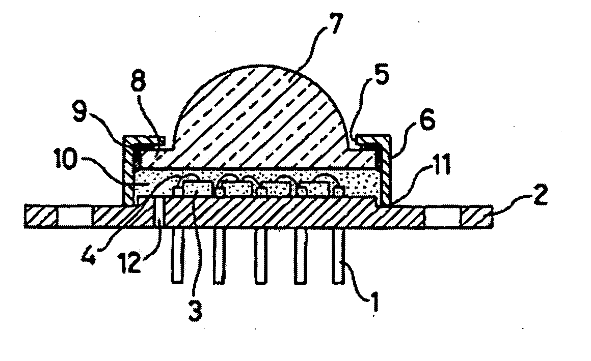
[0045]FIG. 4 is a top view illustrating an exemplary embodiment of an LED device made in accordance with principles of the invention, and FIG. 5 is a cross-sectional view taken along line A-A of FIG. 4. A plurality of leads 1 made of a conductive material can extend out from a stem 2, and an LED chip 3 (or a plurality of LED chips 3) can be mounted with high density on the stem 2 via a conductive adhesive material or other attachment structure or material. A lower electrode of each of the LED chips 3 can be electrically connected with the s...


PUM


Abstract

An LED device can include LED chips mounted with high density and encapsulated with a resin. The device may not be substantially affected by fluctuations in thermal stress generated in the encapsulating resin and can have reduced fluctuations in characteristics such as output power and a color tone and can have a high level of reliability which can be maintained over a long period of time. The LED device can be manufactured by a method that includes mounting LED chips with high density on a metal stem having conductive-material-made leads that extend from the metal stem, welding a lens holder having a lens temporarily fixed thereto by a silicone resin to the stem so as to enclose the LED chips, and encapsulating the LED chips and bonding wires by injecting a silicone resin serving as an encapsulating resin having translucency and flexibility into a space defined by the stem, the holder, and the lens.

Description

[0001] This application claims the priority benefit under 35 U.S.C. §l 119 of Japanese Patent Application No. 2004-327878 filed on Nov. 11, 2004, which is hereby incorporated in its entirety by reference. BACKGROUND OF THE INVENTION [0002] 1. Field of the Invention [0003] The invention relates to an LED device emitting high power and / or multicolor light by mounting at least one LED chip and to a method for manufacturing the same. [0004] 2. Description of the Related Art [0005] A light emitting diode (LED) is a light emitting element made of semiconductor materials and is formed by joining a p-type semiconductor and an n-type semiconductor. The light emission principle of an LED is that a bias voltage is applied in the forward direction to convert electrical energy to light energy at the junction (an active layer). The peak light emission wavelength of an LED depends on the semiconductor materials, but falls within the wavelength range of ultra violet rays via visible rays to infrare...

Claims


Application Information

Patent Timeline
IPC IPC(8): H01L33/00H01L33/58H01L33/62
CPCH01L25/0753H01L33/483H01L33/58H01L2224/48091H01L2924/00014H01L2924/00
Inventor IWASAKI, KAZUYUKISUZUKI, FUSAO
Owner STANLEY ELECTRIC CO LTD
Features
  • Generate Ideas
  • Intellectual Property
  • Life Sciences
  • Materials
  • Tech Scout
  • Unparalleled Data Quality
  • Higher Quality Content
  • 60% Fewer Hallucinations
Learn More