CMOS image sensor

a metal oxide semiconductor and image sensor technology, applied in the direction of semiconductor devices, electrical equipment, radio frequency control devices, etc., can solve the problems of low image quality large variance in the distribution of impurities in pixels or wafers, and estimated less efficiency of cmos image sensors, so as to improve charge transfer efficiency and signal gain, reduce the variance of characteristics among pixels or wafers, the effect of improving the efficiency of charge transfer

Inactive Publication Date: 2006-05-25
SONG YOUNG JOO +2
View PDF1 Cites 137 Cited by
  • Summary
  • Abstract
  • Description
  • Claims
  • Application Information

AI Technical Summary

Benefits of technology

[0014] The present invention is directed to a CMOS image sensor including a pinned photodiode, which can improve charge transfer efficiency and a signal gain and reduce the variance of the characteristics among pixels or wafers so that the CMOS image sensor can have better performance.

Problems solved by technology

Nevertheless, the CMOS image sensor is estimated to be less efficient than the CCD because of several problems.
A low performance of the CMOS image sensor arises from a low signal-to-noise ratio (SNR) and a low dynamic range (DR), and the distribution of the SNR and DR among pixels or wafers is unstable to cause low image quality in the CMOS image sensor.
Also, a variance in the distribution of impurities in pixels or wafers is relatively large.

Method used


Image

  • CMOS image sensor
  • CMOS image sensor
  • CMOS image sensor

Examples


Embodiment Construction

[0026] The present invention will now be described more fully hereinafter with reference to the accompanying drawings, in which exemplary embodiments of the invention are shown. This invention may, however, be embodied in different forms and should not be construed as limited to the embodiments set forth herein. Rather, these embodiments are provided so that this disclosure is thorough and complete and fully conveys the scope of the invention to those skilled in the art.

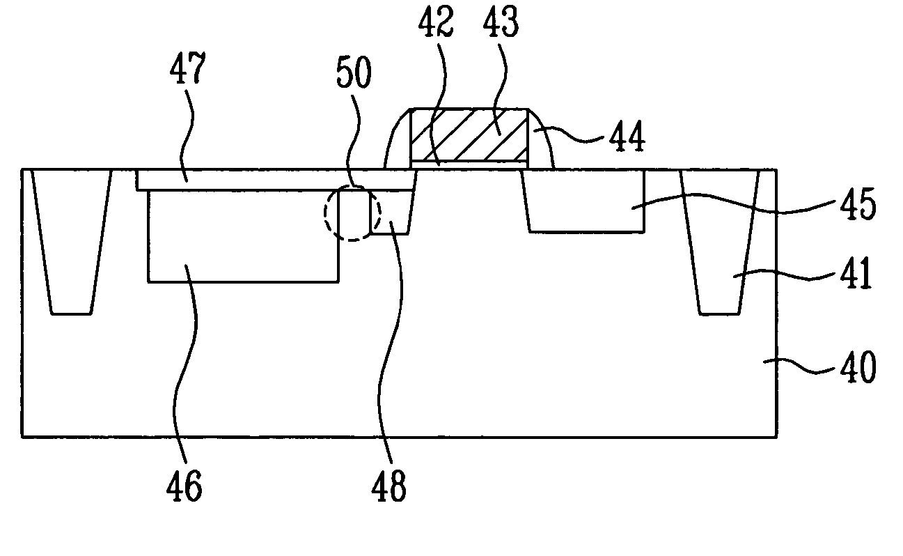
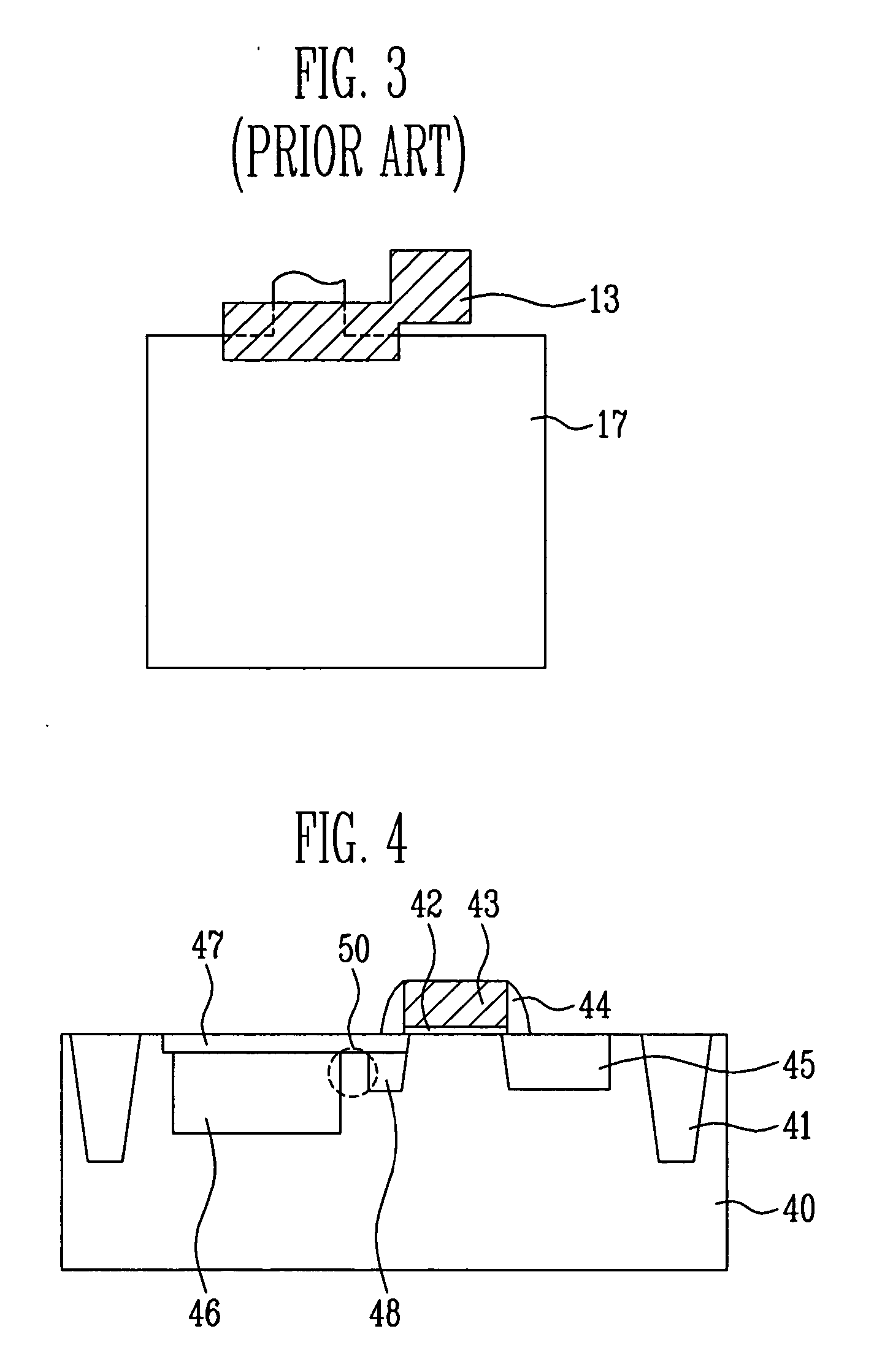
[0027] According to the present invention, in a CMOS image sensor including a pinned photodiode and a transfer transistor, a portion that connects a source of the transfer transistor and the pinned photodiode (hereinafter, a connection portion) is structurally modified in order to improve charge transfer efficiency and a signal gain and greatly reduce the variance of the characteristics among pixels or wafers.

[0028]FIG. 4 is a cross-sectional view of a CMOS image sensor according to an exemplary embodiment of the p...


PUM


Abstract

Provided is a CMOS image sensor including a pinned photodiode and a transfer transistor. The CMOS image sensor includes: a substrate; a gate electrode disposed on the substrate and electrically isolated from the substrate by a gate insulating layer; a first floating region disposed in the substrate of one side of the gate electrode; a first impurity region for a photodiode disposed in the substrate of the other side of the gate electrode; a second floating region disposed in the substrate between the first impurity region for the photodiode and the gate electrode; and a second impurity region for the photodiode disposed in a surface portion of the substrate including the first impurity region for the photodiode and the second floating region.

Description

CROSS-REFERENCE TO RELATED APPLICATION [0001] This application claims priority to and the benefit of Korean Patent Application No. 2004-97659, filed Nov. 25, 2004, the disclosure of which is incorporated herein by reference in its entirety. BACKGROUND [0002] 1. Field of the Invention [0003] The present invention relates to a complementary metal oxide semiconductor (CMOS) image sensor and, more specifically, to a CMOS image sensor including a pinned photodiode and a transfer transistor. [0004] 2. Discussion of Related Art [0005] In general, a CMOS image sensor is a semiconductor device that converts optical images into electric signals and is composed of a photodiode and a circuit block for processing signals. [0006]FIG. 1 is a schematic circuit diagram of a typical CMOS image sensor. Referring to FIG. 1, the CMOS image sensor includes a photodiode 1, a transfer transistor 2, a reset transistor 4, a drive transistor 5, a select transistor 6, and a load transistor 7. The photodiode 1 ...

Claims


Application Information

Patent Timeline
Patent Type & Authority Applications(United States)
IPC IPC(8): H01L27/148
CPCH01L27/14601H01L27/14603H01L27/146
Inventor SONG, YOUNG JOOMHEEN, BONG KIKANG, JIN YEONG
Owner SONG YOUNG JOO
Why Eureka
Try Eureka