
Reduced power magnetoresistive random access memory elements

Inactive Publication Date: 2006-05-25
EVERSPIN TECHNOLOGIES
View PDF99 Cites 23 Cited by
  • Summary
  • Abstract
  • Description
  • Claims
  • Application Information

AI Technical Summary

Problems solved by technology

Large bit and digit line currents are undesirable because memory array power consumption is a serious limiting factor in MRAM applications.
This may result in larger, more expensive MRAM devices.

Method used


Image

  • Reduced power magnetoresistive random access memory elements
  • Reduced power magnetoresistive random access memory elements
  • Reduced power magnetoresistive random access memory elements

Examples


Embodiment Construction

[0021] The following detailed description of the invention is merely exemplary in nature and is not intended to limit the invention or the application and uses of the invention. Furthermore, there is no intention to be bound by any theory presented in the preceding background of the invention or the following detailed description of the invention.

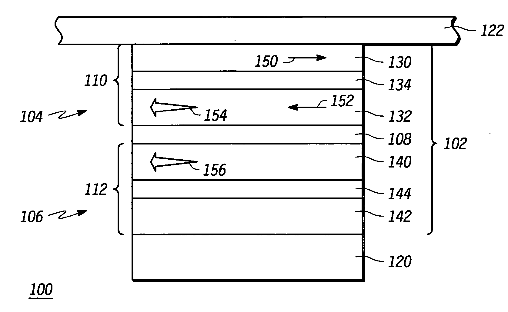
[0022] Turning now to FIG. 3, in accordance with an exemplary embodiment of the present invention, a simplified sectional view of an MRAM array 100 comprises a scalable magnetoresistive memory element 102. In this illustration, only a single magnetoresistive memory element 102 is shown for simplicity in describing the embodiments of the present invention, but it will be understood that MRAM array 100 may consist of a number of magnetoresistive memory elements 102.

[0023] Magnetoresistive memory element 102 is sandwiched between a bit line 122 and a digit line 120. Bit line 122 and digit line 120 include conductive material such that a curr...


PUM


Abstract

Low power magnetoresistive random access memory elements and methods for fabricating the same are provided. In one embodiment, a magnetoresistive random access device has an array of memory elements. Each element comprises a fixed magnetic portion, a tunnel barrier portion, and a free SAF structure. The array has a finite magnetic field programming window Hwin represented by the equation Hwin≈(Hsat−Nσsat)−(Hsw+Nσsw), where Hsw is a mean switching field for the array, Hsat is a mean saturation field for the array, and Hsw for each memory element is represented by the equation HSW≅√{square root over (HkHSAT)}, where Hk represents a total anisotropy and HSAT represents an anti-ferromagnetic coupling saturation field for the free SAF structure of each memory element. N is an integer greater than or equal to 1. Hk, HSAT, and N for each memory element are selected such that the array requires current to operate that is below a predetermined current value.

Description

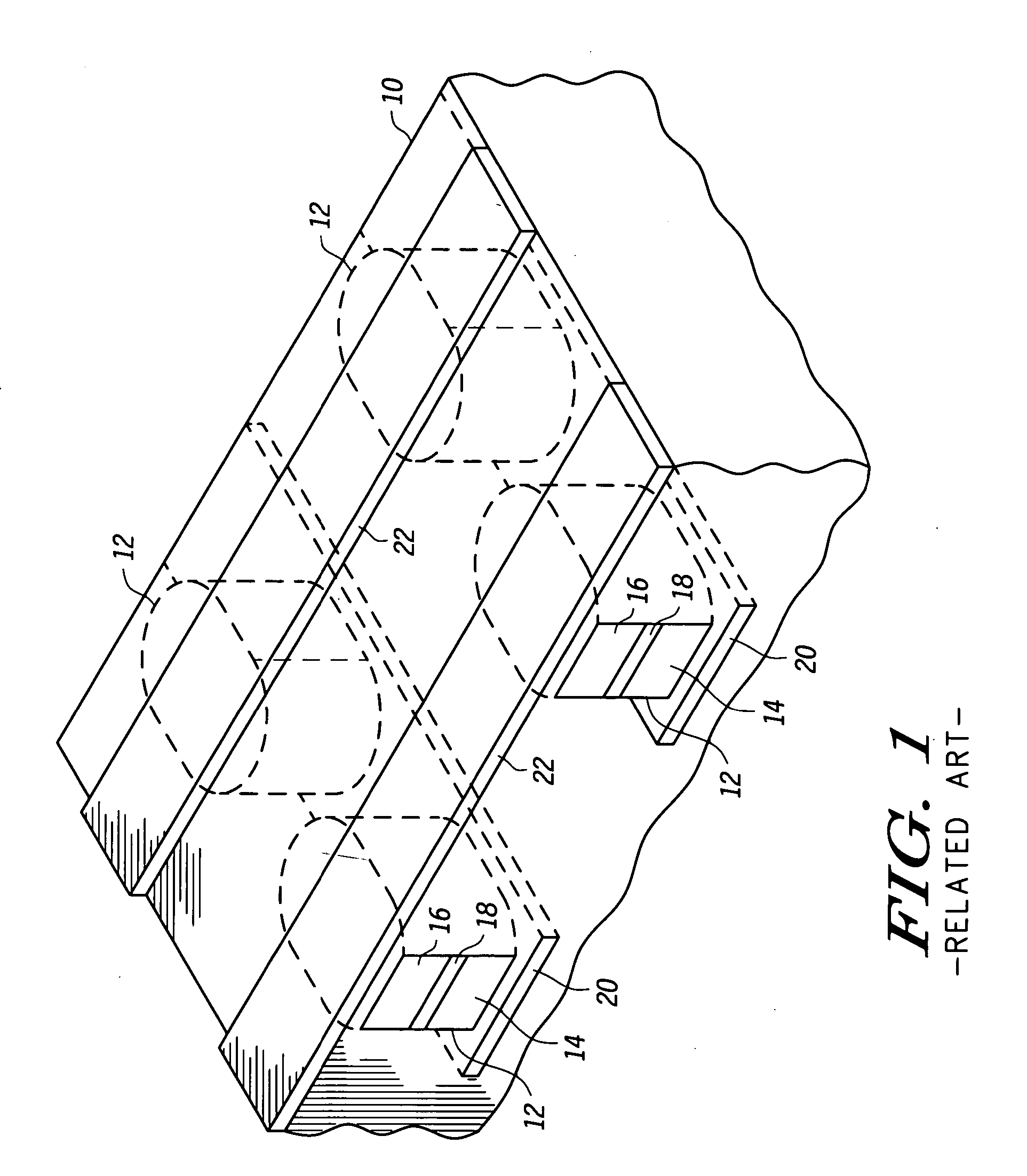
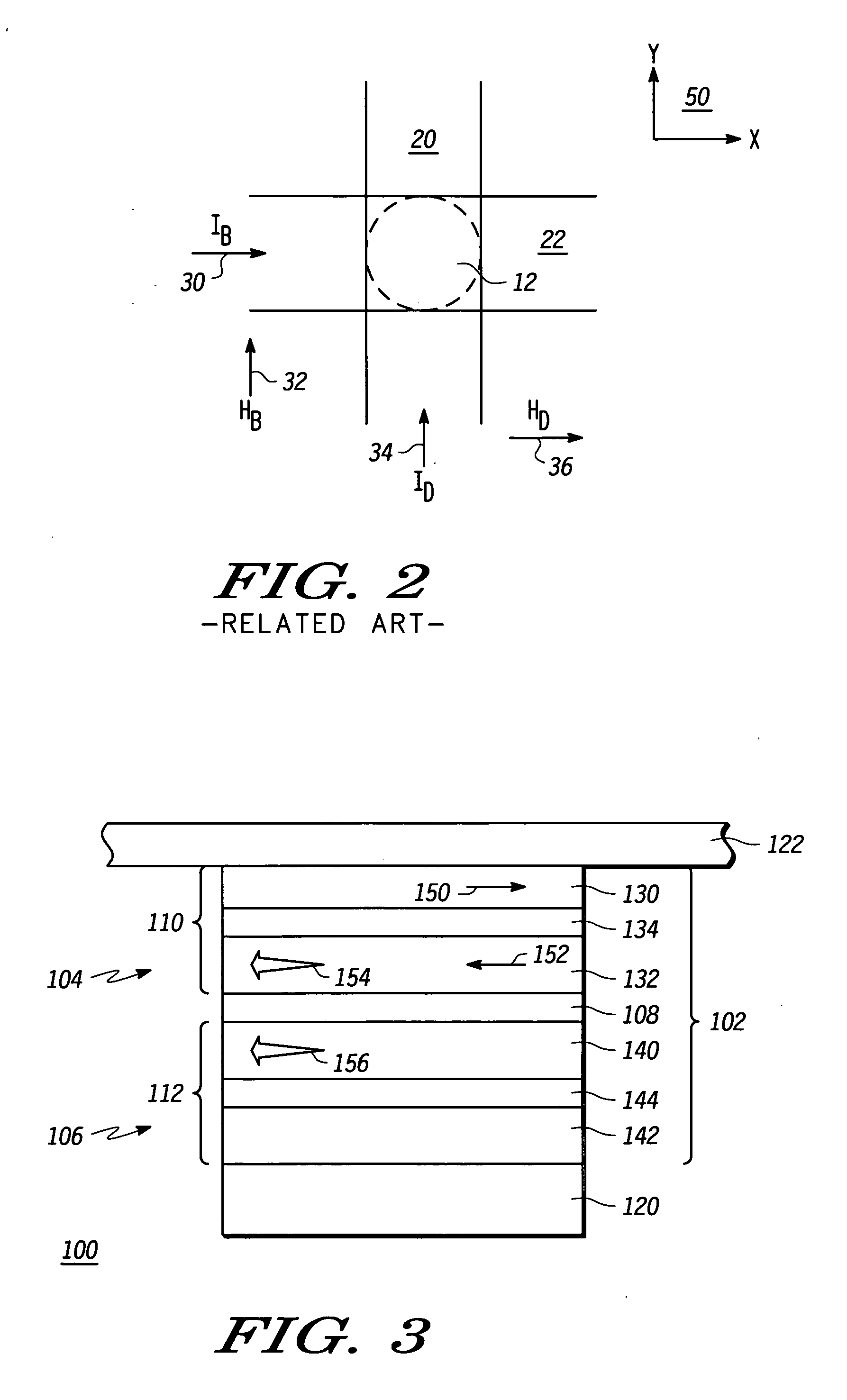
FIELD OF THE INVENTION [0001] The present invention generally relates to magnetoelectronic devices, and more particularly relates to magnetoresistive random access memory elements that require lower power for operation. BACKGROUND OF THE INVENTION [0002] Magnetoelectronic devices, spin electronic devices, and spintronic devices are synonymous terms for devices that make use of effects predominantly caused by electron spin. Magnetoelectronics is used in numerous information devices, and provides non-volatile, reliable, radiation resistant, and high-density data storage and retrieval. The numerous magnetoelectronics information devices include, but are not limited to, Magnetoresistive Random Access Memory (MRAM), magnetic sensors, and read / write heads for disk drives. [0003] Typically, a magnetoelectronic information device, such as an MRAM, includes an array of memory elements. Each memory element typically has a structure that includes multiple magnetic layers separated by various n...

Claims


Application Information

Patent Timeline
IPC IPC(8): H01L29/94
CPCG11C11/16H01L27/222H01L43/08H10B61/00H10N50/10G11C11/15H01L27/10
Inventor RIZZO, NICHOLAS D.DAVE, RENU W.ENGEL, BRADLEY N.JANESKY, JASON A.SUN, JIJUN
Owner EVERSPIN TECHNOLOGIES
Learn More