Semiconductor device and method of fabricating the same
a technology of semiconductor devices and semiconductors, applied in semiconductor devices, semiconductor/solid-state device details, electrical apparatus, etc., can solve the problems of relatively long fabrication period, and relative large number of steps, so as to reduce the fabrication period and cost, and the manufacturing process can be further simplified.
- Summary
- Abstract
- Description
- Claims
- Application Information
AI Technical Summary
Benefits of technology
Problems solved by technology
Method used
Image

Examples
first embodiment
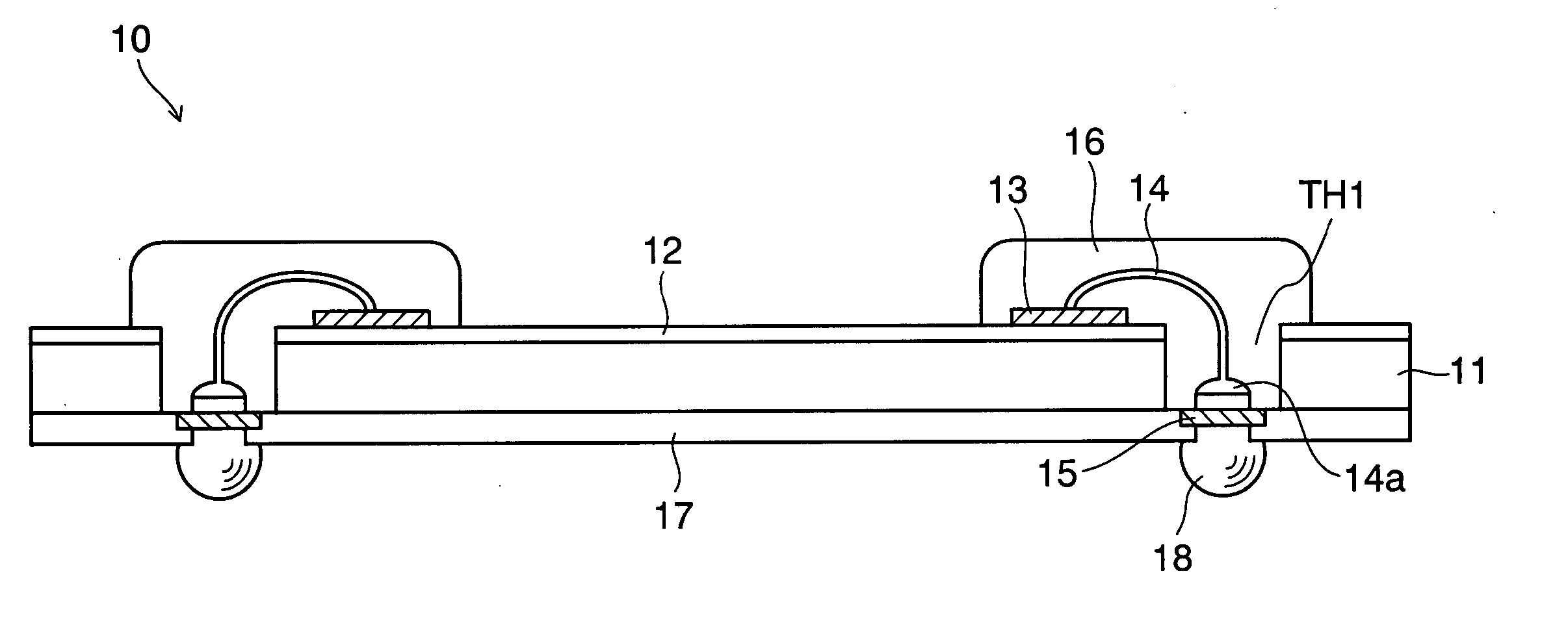
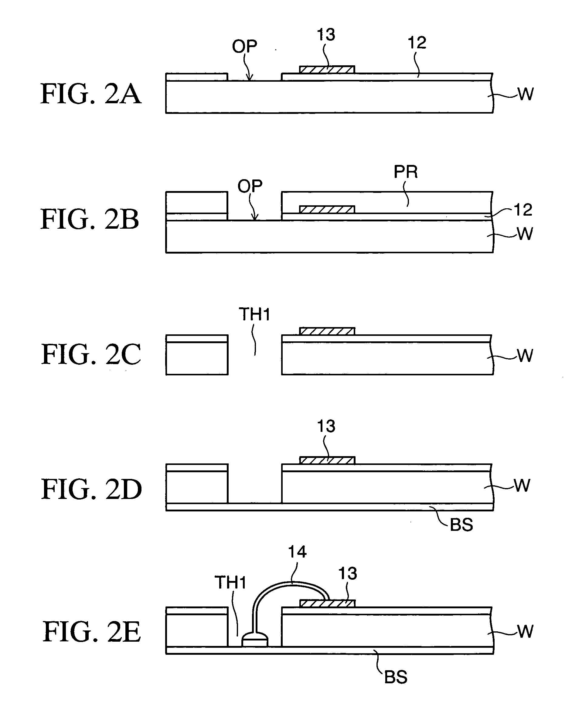
[0029]FIG. 1 schematically illustrates, in a cross-sectional view, the structure of a semiconductor device according to the present invention.
[0030] The semiconductor device 10 according to this embodiment basically has a structure in which portions above and under through holes TH1 formed at predetermined positions in the silicon substrate 11 as illustrated in this drawing are connected by wire bonding via the through holes TH1. Furthermore, the semiconductor device 10 has the feature that it is possible to form a multilayered stack or to mount another chip component, a semiconductor device, or the like on the semiconductor device 10 using pads (conductor layer) or external connection terminals exposed from a protective film when necessary as described later.
[0031] The silicon substrate 11 corresponds to part of a wafer which is ultimately obtained by dividing the silicon wafer having a plurality of functional elements (devices) formed therein in advance into individual chips as d...
second embodiment
[0057]FIG. 5 schematically illustrates, in a cross-sectional view, the structure of a semiconductor device according to the present invention.
[0058] Similar to the semiconductor device 10 (FIG. 1) according to the first embodiment, the semiconductor device 10a according to the second embodiment includes a structure (structure in which portions above and under through holes TH2 formed at predetermined positions in a device formation region are connected via the through holes TH2 by wire bonding) which characterizes the present invention.
[0059] In comparison with the case of the first embodiment (FIG. 1), the difference in structure is that the surface (i.e., the surface of the silicon substrate 11 in which a functional element (device) is formed) on which the passivation film 12 is formed is placed on the vertically opposite side to that in the case of the first embodiment (FIG. 1) and covered with the solder resist layer 17. Accordingly, the pad 13 to which one end of the bonding w...
third embodiment
[0070]FIG. 8 schematically illustrates, in a cross-sectional view, the structure of a semiconductor device according to the present invention.
[0071] Similar to the semiconductor devices 10 and 10a (FIGS. 1 and 5) according to the aforementioned first and second embodiments, the semiconductor device 50 according to this third embodiment includes the structure (structure in which portions above and under through holes TH3, TH4, and TH5 formed at predetermined positions in a device formation region are connected via the through holes TH3, TH4, and TH5 by wire bonding) which characterizes the present invention.
[0072] In comparison with the case of the first and second embodiments (FIGS. 1 and 5), the difference in structure is that two semiconductor chips (semiconductor devices 10b and 10c) are stacked in two layers with an adhesive layer 51 interposed therebetween. The structure of the lower chip (semiconductor device 10b) is basically the same as that for the case of the second embod...
PUM
 Abstract
Description
Claims
Application Information
 - R&D
- Intellectual Property
- Life Sciences
- Materials
- Tech Scout
- Unparalleled Data Quality
- Higher Quality Content
- 60% Fewer Hallucinations
Browse by: Latest US Patents, China's latest patents, Technical Efficacy Thesaurus, Application Domain, Technology Topic, Popular Technical Reports.
© 2025 PatSnap. All rights reserved.Legal|Privacy policy|Modern Slavery Act Transparency Statement|Sitemap|About US| Contact US: help@patsnap.com