Programmable logic cell
a logic cell and a technology of a logic cell, applied in the field of programmable logic cells, can solve the problems of increasing power requirements, fpga has long time delays and increased power requirements, and fpga or a logic cell used for performing arithmetic functions, etc., and achieves the effects of reducing the number of boolean functions, compact form, and reducing energy consumption
- Summary
- Abstract
- Description
- Claims
- Application Information
AI Technical Summary
Benefits of technology
Problems solved by technology
Method used
Image

Examples
first embodiment
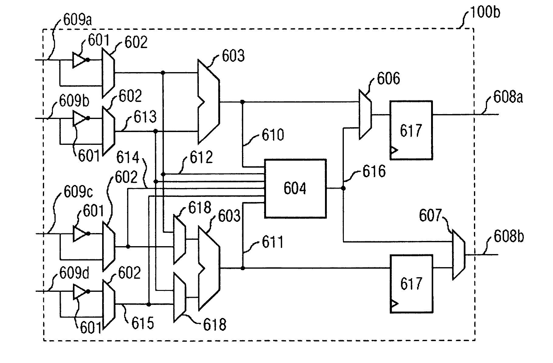
[0050]FIG. 4 shows a logic cell 100b. The logic cell 100b has four inputs 609a-d and two outputs 608a-b. Each input 609a-d is fed to a selection inversion logic 601, 602, which includes in each case of an inverter 601 and a multiplexer 602 and ensures that the respective input 609a-d is fed to a remainder of the logic cell 100b via an additional logic (not shown) of the logic cell 100b, configurably inverted or not inverted. The two inputs 609a-b are fed inverted or not inverted to a first (in FIG. 4 above) 1-bit ALU 603 while via the additional logic with the help of two multiplexers 618 it is configurable whether the inputs 609a-b or the inputs 609c-d are fed inverted or not inverted to a second (in FIG. 4 below) 1-bit ALU 603. A block generator 604 has six inputs 610-615 and one output 616. The six inputs 610-615 are made up of one output 610 from the first 1-bit ALU, one output 611 from the second 1-bit ALU and the four outputs 612-615 from the multiplexers 602 of the selection ...
second embodiment
[0060]FIG. 10 shows a logic cell 100c, which differs from the logic cell 100b shown in FIG. 4 only in the input area and in the 1-bit ALUs 1101 which are used. While for the logic cell 100b both inputs of both 1-bit ALUs 603 can be inverted with the respective selection inversion logic 601, 602, for the logic cell 100c shown in FIG. 10 only one input in each case of the two 1-bit ALUs 1101 can be inverted with the respective selection inversion logic 601, 602. The remaining reference labels correspond to those of the logic cell 100b in FIG. 4.
[0061] Since it is not possible for both inputs of the 1-bit ALU in the logic cell 100c to be inverted, a 1-bit ALU 1101 usable for the logic cell 100c must have a function other than that of the 1-bit ALU 603 or the 1-bit ALU 603′. The 1-bit ALU 1101 is represented in FIG. 11. In construction, the 1-bit ALU 1101 is similar to the 1-bit ALU 603 shown in FIG. 7, and for that reason only the differences are explained here. The 1-bit ALU 1101 addi...
third embodiment
[0064]FIG. 12 represents a logic cell 100d. None of the inputs 609a-d of the logic cell 100d can be inverted. Consequently none of the previously described 1-bit ALUs 603, 603′, 1101 can be used for the logic cell 100d. For this reason, a 1-bit ALU 1403 which is represented in FIG. 13 is used in the logic cell 100d.
[0065] Compared to the 1-bit ALU 1101, the 1-bit ALU 1403 additionally contains an inverter 1500, a NAND gate 1501 with an inverted input and an AND gate 1502 with an inverted input. The input of the inverter 1500 and the inverted input of the NAND gate 1501 and of the AND gate 1502 are connected to the same input 1401b of the 1-bit ALU 1403. The output of the inverter, the output of the NAND gate 1501 with inverted input and the output of the AND gate 1502 with inverted input is connected in each case via a tri-state driver 11 to the output 1402 of the 1-bit ALU. These three additional gates 1500-1502 replace the absent selection inversion logic in the logic cell 100d. ...
PUM
 Abstract
Description
Claims
Application Information
PatSnap Eureka turns technology decisions into work you can execute. Powered by our Innovation Knowledge Graph, it runs expert workflows across engineering, life sciences, materials and intellectual property. Get your review-ready output in minutes.


